
- Sopto Home

- Fiber Optic Transceiver Module
-
- 10G 1310nm 10km X2 LR SPT-X2-LR
- Fiber Optic Transceiver Module
- High Speed Cable
- Fiber Optical Cable
- Fiber Optical Patch Cords
- Splitter CWDM DWDM
- PON Solution
- FTTH Box ODF Closure
- PCI-E Network Card
- Network Cables
- Fiber Optical Adapter
- Fiber Optical Attenuator
- Fiber Media Converter
- PDH Multiplexers
- Protocol Converter
- Digital Video Multiplexer
- Fiber Optical Tools
- Compatible


- 1.25G & 125M Transceiver
- 100G QSFP28 Transceiver
- 100G/40G/25G
- 10G Transceiver
- 10G X2 Transceiver
- Copper SFP Transceiver
- CPRI LTE SFP Transceiver
- Fiber Channel & SDH
- MiniGBIC/SFP Transceiver
- PON Transceiver
- Video SFP Transceiver
- WDM XFP
- SGMII 100BASE FX SFP
- Gigabit Interface Converter
- Video SFP
- 40G QSFP+ Transceiver
- WDM SFP
- CWDM SFP
- DWDM SFP
- WDM SFP+
- 10G SFP+ Transceiver
- CWDM SFP+
- DWDM SFP+
- 10G XFP
- CWDM XFP
- DWDM XFP
- WDM SFF
- 10G XENPAK
- CWDM XENPAK
- DWDM XENPAK
- WDM GBIC
- CWDM X2
- DWDM X2
- GBIC Copper
- CSFP Transceiver
- CFP Transceiver
- GPON SFP Transceiver
- 1X9 Transceiver
- GEPON SFP Transceiver


10G 1310nm 10km X2 LR SPT-X2-LR

Features
- Compatible with X2 MSA Rev2.0b
- Support of IEEE 802.3ae 10GBASE-LR at 10.3125Gbps
- Transmission Distance up to 10Km(SMF)
- SC Receptacle 1310 DFB Laser
- SC Duplex Optical Connector
- Hot Pluggable 70-PIN Connector with XAUI Electrical Interface
- Management and control via MDIO 2-wire interface
- Power Supply :+3.3V, APS(+1.2V)
- Diagnostic Optics Monitoring
- Temperature Range: 0~ 70 °C
- ROHS Compatible
Applications
- 10GE Ethernet switches and routers
- 10GE Core-routers
- 10GE Storage
- Other 10Gbps Ethernet Transmission System
Product Description
The SPT-X2-LR is a highly integrated、Serial optical transponder module for high-speed, 10Gbit/s data transmission applications. 4×3.125Gbps Ethernet Signal Input by XAUI Interface. An integrated Coder / Decoder and multiplexer / de multiplexer (SERDES: Serializer / Deserializer). Designing for 300m Transmission with a vertical cavity surface emitting laser (VCSEL) Digital diagnostics functions are available via a 2-wire serial interface, as specified in the XENPAK MSA 3.0.
Absolute Maximum Ratings
|
Parameter |
Symbol |
Min |
Max |
Unit |
Ref. |
|
Storage Ambient Temperature Range |
|
-40 |
+85 |
°C |
non condensing |
|
Powered case Temperature Range |
|
0 |
+70 |
°C |
non condensing |
|
Adaptable Power Supply (APS) |
Vapsense |
0 |
1.5 |
V |
Voltage @ Pin APS Sense |
|
Supply Voltage Range @ 3.3V |
Vcc3 |
-0.5 |
4.0 |
V |
|
Any stress beyond the maximum ratings can result in permanent damage. The device specifications are guaranteed only under the recommended operating conditions.
Recommended Operating Conditions
|
Parameter |
Symbol |
Min |
Typical |
Max |
Unit |
|
|
Operating Case Temperature |
Tc |
0 |
|
+70 |
°C |
|
|
Power Supply Voltage |
|
VCC3 |
3.14 |
3.0 |
3.47 |
V |
|
|
VAPS |
1.152 |
1.2 |
1.248 |
||
|
Power Dissipation |
PD |
|
3.5 |
4 |
W |
|
XAUI I/O Characteristics
|
Parameter |
Symbol |
Min. |
Typ. |
Max. |
Unit |
Note |
|
XAUI Date Rate |
DR |
|
3.125 |
|
Gb/s |
|
|
XAUI Baud Rate Tolerance |
|
-100 |
|
+100 |
ppm |
Relative Tolerance |
|
Differential Input Voltage Swing |
|
220 |
|
1600 |
mv |
8B/10B Coded Input Signal |
|
Differential Output Voltage Swing |
|
800 |
|
1600 |
mVp-p |
RLOAD = 100Ω ± 5% |
|
Differential Input Impedance |
|
80 |
100 |
120 |
Ω |
|
|
Total Output Jitter |
TJXAUI |
|
|
0.35 |
UI |
no pre-equalization |
|
Total Deterministic Output Jitter |
DJXAUI |
|
|
0.17 |
UI |
no pre-equalization |
Optical Interface
Transmitter Characteristics
|
Parameter |
Symbol |
Min. |
Typ. |
Max. |
Unit |
Note |
|
Operating Range |
|
|
|
10 |
Km |
|
|
Operating Date Rate |
|
|
10.3125 |
|
Gb/s |
|
|
Overload |
Po |
-8.2 |
|
0.5 |
dBm |
|
|
Input Centre Wavelength |
λ |
1260 |
1310 |
1255 |
nm |
|
|
SMSR. |
SWSR |
30 |
|
|
dB |
|
|
Extinction Ratio |
ER |
3.5 |
6 |
|
|
|
|
Optical Modulation Amplitude |
OMA |
500 |
|
|
µW |
|
|
Transmitter and Dispersion Penalty |
TDP |
|
|
3.2 |
dB |
|
Receiver Characteristics
|
Parameter |
Symbol |
Min. |
Typ. |
Max. |
Unit |
Note |
|
Operating Date Rate |
|
|
10.3125 |
|
Gb/s |
|
|
Overload |
Po |
0.5 |
|
|
dBm |
|
|
Sensitivity in OMA |
OMA0 |
|
|
-12.6 |
dBm |
|
|
Stressed Sensitivity in OMA |
OMAst |
|
|
-10.3 |
dBm |
|
|
Sensitivity MINI |
Pmin |
|
|
-14.4 |
dBm |
1 |
Note: 1. Measured at 10.3125Gb/s,Non-framed PRBS2 31-1,NRZ
Electrical PAD Layout
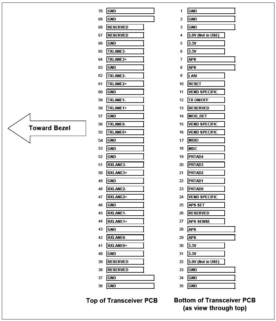
Host PCB X2 PINOUT
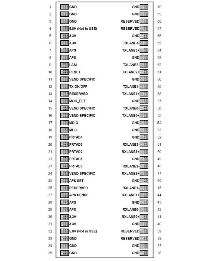
Pin Descriptions
|
PIN NO |
Name |
Dir |
Logic |
Function |
|
1 |
GND |
|
|
Electrical Ground |
|
2 |
GND |
|
|
Electrical Ground |
|
3 |
GND |
|
|
Electrical Ground |
|
4 |
5.0V |
|
|
Power |
|
5 |
3.3V |
|
|
Power |
|
6 |
3.3V |
|
|
Power |
|
7 |
APS |
|
|
Adaptive Power Supply |
|
8 |
APS |
|
|
Adaptive Power Supply |
|
9 |
LASI |
O |
1.2V CMOS Open Drain |
Link Alarm Status Interrupt, low active, Open Drain Output A pull-up resistor with 10-22KΩ to 1,2V is expected. Logic High: Normal Operation Logic Low: Link Alarm is indicated |
|
10 |
Reset |
I |
1.2V CMOS Open Drain |
Low active Reset Input 10KΩ pull-up on Transceiver Logic high = Normal Operation Logic Low = Reset asserted |
|
11 |
VEND SPECIFIC |
|
|
Vendor Specific Pin,. leave unconnected |
|
12 |
TX ON/OFF |
I |
1.2V CMOS Open Drain |
High active Transmitter Enable Input 10KΩ pull-up on Transceiver Logic high = Transmitter active (normal Operation) And Register Bit 1.9.0 set to low as well Logic Low = shut down of Transmitter |
|
13 |
RESERVED |
|
|
RESERVED |
|
14 |
MOD DETECT |
O |
|
1kΩ to Ground On Transceiver |
|
15 |
VEND SPECIFIC |
|
|
Vendor Specific Pin,. leave unconnected |
|
16 |
VEND SPECIFIC |
|
|
Vendor Specific Pin,. leave unconnected |
|
17 |
MDIO |
I/O |
1.2V CMOS |
Management Data I/O. Requires external 10-22 kΩ pull- up to 1.2 V on host. |
|
18 |
MDC |
I |
1.2V CMOS |
Management Clock Input |
|
19 |
PRTAD4 |
I |
|
Port Address Bit 4(LOW=0) |
|
20 |
PRTAD3 |
I |
|
Port Address Bit 3(LOW=0) |
|
21 |
PRTAD2 |
I |
|
Port Address Bit 2(LOW=0) |
|
22 |
PRTAD1 |
I |
|
Port Address Bit 1(LOW=0) |
|
23 |
PRTAD0 |
I |
|
Port Address Bit 0(LOW=0) |
|
24 |
VEND SPECIFIC |
|
|
Vendor Specific Pin,. leave unconnected |
|
25 |
APS SET |
I |
|
Feedback Input for APS, Input of APS Setting Resistor |
|
26 |
RESERVED |
|
|
RESERVED |
|
27 |
APS SENSE |
O |
|
APS Sense Output for APS Control Circuit |
|
28 |
APS |
|
|
Adaptive Power Supply |
|
29 |
APS |
|
|
Adaptive Power Supply |
|
30 |
3.3V |
|
|
Power |
|
31 |
3.3V |
|
|
Power |
|
32 |
5.0V |
|
|
Power |
|
33 |
GND |
|
|
Electrical Ground |
|
34 |
GND |
|
|
Electrical Ground |
|
35 |
GND |
|
|
Electrical Ground |
|
36 |
GND |
|
|
Electrical Ground |
|
37 |
GND |
|
|
Electrical Ground |
|
38 |
RESERVED |
|
|
RESERVED |
|
39 |
RESERVED |
|
|
RESERVED |
|
40 |
GND |
|
|
Electrical Ground |
|
41 |
RX LANE 0+ |
|
|
Module XAUI Output Lane 0+ |
|
42 |
RX LANE 0- |
|
|
Module XAUI Output Lane 0- |
|
43 |
GND |
|
|
Electrical Ground |
|
44 |
RX LANE 1+ |
|
|
Module XAUI Output Lane 1+ |
|
45 |
RX LANE 1- |
|
|
Module XAUI Output Lane 1- |
|
46 |
GND |
|
|
Electrical Ground |
|
47 |
RX LANE 2+ |
|
|
Module XAUI Output Lane 2+ |
|
48 |
RX LANE 2- |
|
|
Module XAUI Output Lane 2- |
|
49 |
GND |
|
|
Electrical Ground |
|
50 |
RX LANE 3+ |
|
|
Module XAUI Output Lane 2+ |
|
51 |
RX LANE 3- |
|
|
Module XAUI Output Lane 2- |
|
52 |
GND |
|
|
Electrical Ground |
|
53 |
GND |
|
|
Electrical Ground |
|
54 |
GND |
|
|
Electrical Ground |
|
55 |
RX LANE 0+ |
|
|
Module XAUI Output Lane 0+ |
|
56 |
RX LANE 0- |
|
|
Module XAUI Output Lane 0- |
|
57 |
GND |
|
|
Electrical Ground |
|
58 |
TX LANE 1+ |
|
|
Module XAUI Output Lane 1+ |
|
59 |
TX LANE 1- |
|
|
Module XAUI Output Lane 1- |
|
60 |
GND |
|
|
Electrical Ground |
|
61 |
TX LANE 2+ |
|
|
Module XAUI Output Lane 2+ |
|
62 |
TX LANE 2- |
|
|
Module XAUI Output Lane 2- |
|
63 |
GND |
|
|
Electrical Ground |
|
64 |
TX LANE 3+ |
|
|
Module XAUI Output Lane 2+ |
|
65 |
TX LANE 3- |
|
|
Module XAUI Output Lane 2- |