-

- Sopto Home
-

- Special Topic
-
- Module Knowledge
-
- Structure of the Bidirectional OSA module
Module Knowledge
- Tips for Buying 10G XFP Transceivers
- XFP Transceivers for Telecommunications
- Three Types of Ethernet SFP Transceiver Modules Introduction
- Info about High Density CXP Optical Module
- Multipurpose CFP Optical Modules
- Info about CFP Management Interface
- SFP+ Transceivers Short Range Module Overview
- 3 Reasons Every Network Needs GLC-LH-SM Transceiver
- Is the GLC-SX-MM Transceiver Right for Your Switch?
SOPTO Special Topic
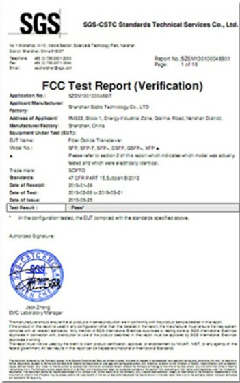
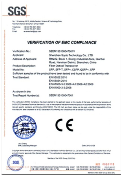
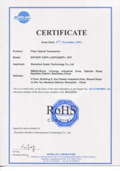
Certificate
Guarantee
Except products belongs to Bargain Shop section, all products are warranted by SOPTO only to purchasers for resale or for use in business or original equipment manufacturer, against defects in workmanship or materials under normal use (consumables, normal tear and wear excluded) for one year after date of purchase from SOPTO, unless otherwise stated...
Return Policies
Defective products will be accepted for exchange, at our discretion, within 14 days from receipt. Buyer might be requested to return the defective products to SOPTO for verification or authorized service location, as SOPTO designated, shipping costs prepaid. .....
Applications
 Fiber Optic Transceiver Modules can be applied to these occasions or fields.
Ethernet
IPTV
FTTX
Security
Video Monitor
SDH/SONET
Data Communication
Storage Area Networks
SNS Page


SOPTO Products
- Fiber Optic Transceiver Module
- High Speed Cable
- Fiber Optical Cable
- Fiber Optical Patch Cords
- Splitter CWDM DWDM
- PON Solution
- FTTH Box ODF Closure
- PCI-E Network Card
- Network Cables
- Fiber Optical Adapter
- Fiber Optical Attenuator
- Fiber Media Converter
- PDH Multiplexers
- Protocol Converter
- Digital Video Multiplexer
- Fiber Optical Tools
- Compatible
Related Products
 10G SFP+ Transceiver
 40G QSFP+ Transceiver
Performance Feature
Stable
Low cost
Small size
Economic
Dust-proof
High speed
Hot-pluggable
Good EMI, EMC
Wide appliaction field
DDM function available
Long transmission distance
Good Anti-static performance
Module Knowledge
Recommended
Structure of the Bidirectional OSA module
Figure 1 shows the structure of the bidirectional OSA module designed in this work. It consists of a vertical-cavity surface-emitting laser (VCSEL), surface-receiving PD and M-PD components, a TRx IC board, and a fiber array. In the TRx IC board, multi-channel Tx and Rx IC chips are die-bonded onto a small printed circuit board (PCB) on which impedance-matched metal traces are formed for an electrical connection with the main board of the TRx module.
VCSEL, PD and M-PD chips are flip-chip bonded onto individual SiOBs, as shown in Fig. 1. These VCSEL, PD and M-PD SiOBs are attached onto an optical fiber array embedded in a V-groove which is formed in a silicon substrate. In the fabrication of these OSA components, we used standard OM3 multi-mode fibers of which the core diameter is 50μm. For the active components, we used commercially available Tx/Rx IC chips and VCSEL/PD arrays.
.png)
Figure 1 Structure of the four-channel bidirectional OSA module:
(a) top-view and (b) cross-sectional view
To couple the PD and the fiber, a 45° mirror (mirror-1) is formed at the end of the fiber, similarly to previous works. However, to couple the VCSEL and fiber, another 45° mirror (mirror-2) having a function of a half-mirror is formed in the fiber. For mirror-2, wavelength-filtering layers are deposited on the polished surface of a fiber segment, and this segment is attached to a 45°-polished main fiber.
Light with a wavelength of 850 nm is emitted from the VCSEL and reflected at mirror-2, after which it enters the fiber for the up-link. Down-linked light with a wavelength of 1060 nm passes through mirror-2 and is reflected at mirror-1, entering into the PD. To monitor the light intensity from the VCSEL, an optical signal leakage window is formed below the M-PD by scratching the fiber to obtain a small amount of scattered light.
.png)
Figure 2 Detailed structure of the SiOB used to package the VCSEL, PD, and M-PD array chips on the fiber array
Figure 2 shows the detailed structure of the SiOB onto which the VCSEL, PD, and M-PD array chips are mounted. Each 1x4 array chip is mounted on a separate SiOB. In the SiOB, a square groove is formed to contain the chip and metal lines are formed on the bottom and side wall of the groove for an electrical connection with the chip. In the SiOB, optical via holes are also formed; the walls of the via holes utilize metal deposited layers to facilitate light transmission through the silicon substrate.
The space between the bottom of the square groove and the PD/VCSEL chip is left as small as possible to reduce any optical crosstalk that could be induced by the divergence and scattering of light beams. When attaching the SiOB to the silicon substrate, alignment marks are formed with copper plating with a thickness of less 8 µm on the SiOB and the silicon substrate. The thickness of the solder ball is less than 5 µm. Thus, the total distance between the SiOB and the silicon substrate is less than 21 µm.
When the fiber is buried in the V-groove formed on the silicon substrate, the distance between the fiber and the SiOB is about 21 µm. In the fabrication of the OSA module, we applied a passive alignment method with these alignment marks. Additionally, the via holes are filled with an index matching oil to reduce scattering at the fiber surface and to maintain the reflection effect of the 45°-mirrors. The diameter of the via holes is 70 µm, which is close to the diameter of the fiber core.
The height of the via holes is 125 µm and the pitch of the via holes and the fibers is 250 µm. In order to place the via holes of the SiOB at the exact position above the mirrors or at the leakage windows of the fiber array, alignment marks are made on the silicon substrate and on the bottom side of the SiOB substrate.
For an efficient alignment of the fibers and the SiOBs we used the following procedure. Four fibers are placed on the V-grooved Si substrate and mounted using an epoxy. This mounted block with the fibers and the Si substrate is polished to make 45° surfaces on both sides. The 45° surfaces are mechanically polished with a deviation of ± 1° using a minute jig and a commercialized polishing machine.
Wavelength-filtering layers are deposited on the polished surfaces of the block. The main fibers to couple to mirror-2 of this block are similarly polished mounting on another V-grooved Si substrate and attached to the block using an index-matching epoxy.
The SiOBs are placed on the Si substrate using align marks made on the Si substrates and the SiOBs. In a ray trace simulation for the geometries of the 850 nm devices and SiOBs, the alignment tolerance to attain a total coupling loss within 3 dB on both the VCSEL and PD sides is about ± 10 μm in the lateral and longitudinal (along the fiber) directions from the central position of the mirrors.
From our alignment procedure, the SiOBs could be placed within ± 3 μm misalignment in the lateral direction and within ± 5 μm in the longitudinal direction, which is expected to be in the range of the 3 dB tolerance for the 850 nm devices. In the rotational angle along the fiber axis, the 45° mirrors can be quite precisely located since the fiber array is already mounted on the Si substrate block and formed the mirrors together.
Notices: This article is reprinted from: opticsinfobase.org/oe/fulltext.cfm?uri=oe-22-2-1768&id=277085
For more, please see next page where we will intro the “Signal transmission in the bidirectional OSA module”. By the way, Sopto supplies high quality fiber optical modules and fiber optical connectors with reasonable price. For the newest quotes, please contact a Sopto representative by calling 86-755-36946668, or by sending an email to info@sopto.com. For more info, please browse our website.
You May Like: