-

- Sopto Home
-

- Special Topic
-
- Module Knowledge
-
- Optical Module Common Problem and Maintenance Method
Module Knowledge
- Tips for Buying 10G XFP Transceivers
- XFP Transceivers for Telecommunications
- Three Types of Ethernet SFP Transceiver Modules Introduction
- Info about High Density CXP Optical Module
- Multipurpose CFP Optical Modules
- Info about CFP Management Interface
- SFP+ Transceivers Short Range Module Overview
- 3 Reasons Every Network Needs GLC-LH-SM Transceiver
- Is the GLC-SX-MM Transceiver Right for Your Switch?
SOPTO Special Topic
Certificate

Guarantee
Except products belongs to Bargain Shop section, all products are warranted by SOPTO only to purchasers for resale or for use in business or original equipment manufacturer, against defects in workmanship or materials under normal use (consumables, normal tear and wear excluded) for one year after date of purchase from SOPTO, unless otherwise stated...
Return Policies
Defective products will be accepted for exchange, at our discretion, within 14 days from receipt. Buyer might be requested to return the defective products to SOPTO for verification or authorized service location, as SOPTO designated, shipping costs prepaid. .....
Applications
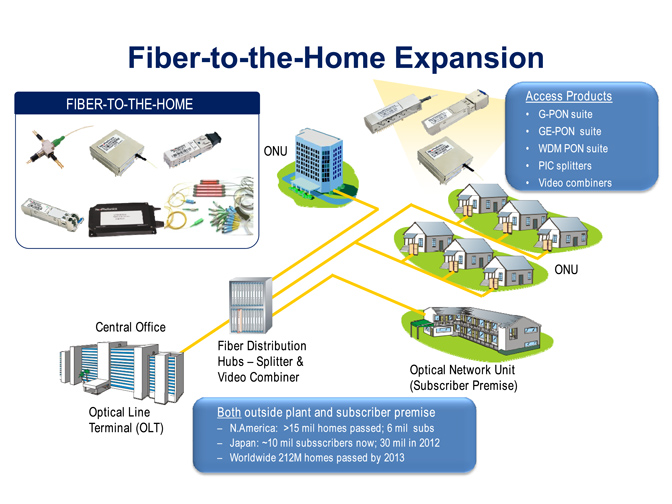 Fiber Optic Transceiver Modules can be applied to these occasions or fields.
Ethernet
IPTV
FTTX
Security
Video Monitor
SDH/SONET
Data Communication
Storage Area Networks
SNS Page


SOPTO Products
- Fiber Optic Transceiver Module
- High Speed Cable
- Fiber Optical Cable
- Fiber Optical Patch Cords
- Splitter CWDM DWDM
- PON Solution
- FTTH Box ODF Closure
- PCI-E Network Card
- Network Cables
- Fiber Optical Adapter
- Fiber Optical Attenuator
- Fiber Media Converter
- PDH Multiplexers
- Protocol Converter
- Digital Video Multiplexer
- Fiber Optical Tools
- Compatible
Related Products
 10G SFP+ Transceiver
 40G QSFP+ Transceiver
Performance Feature
Stable
Low cost
Small size
Economic
Dust-proof
High speed
Hot-pluggable
Good EMI, EMC
Wide appliaction field
DDM function available
Long transmission distance
Good Anti-static performance
Module Knowledge
Recommended
Optical Module Frequently Asked Questions:
Take 1.25G SFP module as an example.
- Optical power badness:
- Eye diagram badness;
- Receiving end badness;
- Working current badness;
- Program Programming failed;
Common-Badness Reason Judging Method
- Visual Method: Check the faulty module appearance. Whether there is obvious damage, component burned black, dehiscence, leakage, even tin or not.
- Comparative Law: Use certain tools and a good module. Test the good module and the target module. Mainly analyze circuit parts or components' resistance, voltage, waveform, etc. Then make a comparison.
- Substitution Method: To replace the components of the module; then to analyze the change of operating parameters.
- Others
Reason and Maintenance methods of common problem of optical module internally
- Optical power badness performance
A1. BIAS optical bias current within the normal range, the optical power exceeds out of the control range.
A2. Laser bias current of BIAS in the normal range, the optical power is less than the control range.
A3. There is no light.
A3.a. BIAS value is displayed as 0.
A3.b. BIAS short circuit, value is very great, displayed as 90mA ~ 150mA; and data can be saved.
A4. There is light during the debug process, but the optical power don't change
A5. Optical power is unstable.
A6. Side mode suppression ratio is small.
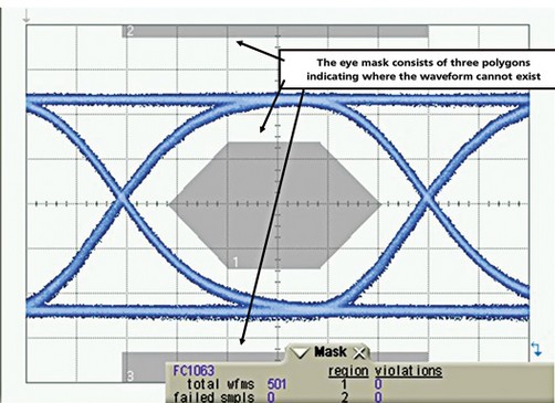
- Eye diagram badness performance
B1. Extinction ratio of non-performing
B1.a Small extinction ratio
B1.b Large extinction ratio
B2. Eye diagram scatter
B3. Graphics irregular
B4. Diagram without eye
- Receiving end badness Performance
C1. Low sensitivity
C2. No sensitivity
C3. Alarm dysfunction
- Working current badness Performance
D1. Open circuit-Operating current is less than 70mA
D2. Operating current is greater than 280mA
D3. Short-circuit-Operating current is greater than 500mA
- Program Programming failed
E1. Program can’t be burnt.
E2. Program can be burnt but without ID
E3. Module or shell is short circuit.
Reason and Maintenance methods:
A1.1 Emission component TOSA is bad.
Maintenance method is to replace the TOSA.
A1.2 The TOSA PINs PD+ is welded badly so that the power is so large. But when debug the software, the power won’t be changed.
Maintenance method is to weld the pin better.
A1.3 Power and resistance don't match with the BIAS optical bias current.
Maintenance method is to improve the power and resistance.
A2.1 Emission component TOSA is bad.
The maintenance method is to replace the TOSA.
A2.2 Paste is bad or poor performance of driver chip.
The repair method is to re-paste driver chip or to replace the chip.
A2.3 Power and resistance don't match with the BIAS optical bias current.
Maintenance method is to reduce the power and resistance.
A3.a.1 The TOSA PINs PD+ is welded badly.
Maintenance method is to weld the pin better.
A3.a.2 Paste is bad or poor performance of storage chip.
The repair method is to re-paste driver chip or to replace the chip.
A3.b.1 The TOSA PINs LD+ is welded badly.
Maintenance method is to weld the pin better.
A3.b.2 Magnetic bead on LD- or LD+ line is bad, drain stickers or mislabeled.
Maintenance method is to reattaching the same type of magnetic beads.
A3.b.3 Paste bad or poor performance of driver chip.
The repair method is to re-paste driver chip or to replace the chip.
A3.b.4 Components of the storage chip pin is bad, drain stickers or mislabeled.
Maintenance method is to reattaching the same type of the component.
A4.1 Emission component TOSA is bad.
Maintenance method is to replace the TOSA.
A4.2 The TOSA PINs LD- is welded badly.
Maintenance method is to weld the pin better.
A5. The cause of the unstable optical power is that the TOSA is bad generally.
To place the TOSA can solve the problem.
A6. The only method is to replace the TOSA.
B1.a One method is to replace the TOSA; the other is to reduce the optical power resistance.
B1.b One method is to replace the TOSA; the other is to improve the optical power resistance.
B2.
①TOSA is bad.
Maintenance method is to replace the TOSA;
② Driver chip performance is bad.
Maintenance method is to change the driver chip;
③Signal impedance mismatch.
Maintenance method is to change the head-end matching resistance.
B3. Modify the value of pull-up resistor, pull-down resistor and the matching resistor.
B4.1
①TOSA is bad.
Replace the TOSA;
②Head-end matching resistor is weld badly or missing stickers.
Maintenance method is to re-paste the same size resistor.
C1.1 ROSA is bad.
Maintenance method is to replace ROSA.
C1.2 ROSA pin OUT+ and OUT- are poorly contacted.
Repair method is to re-weld the pin.
C1.3 Extinction ratio of light source is too small.
The processing is to adjust the extinction ratio to 10 or more.
C1.4 Burn of program is not complete.
Processing method is to burn again.
C1.5 Limiting amplifier chip is bad or poor performance.
Approach is to re-posted or replace limiting amplifier.
C1.6 If the avalanche diode ADP causes the sensitivity low.
Processing method is to adjust to ADP voltage to the best.
C2.1 ROSA is bad.
Maintenance method is to replace ROSA.
C2.2 ROSA pin OUT+ and OUT- are poor welded.
Repair method is to re-weld the pin.
C2.3 The coupling capacitor of OUT+ and OUT- line is even tin.
Maintenance method is to separate the even tin between the capacitances.
C2.4 The magnetic beads is welded badly or leakage stickers.
Processing method is to re-paste the same type of magnetic beads.
C2.5 Limiting amplifier chip is bad or poor performance.
The approach is to re-posted or replace limiting amplifier.
C3.1 The ROSA is bad or the alarm resistor is mismatch.
Processing method is to replace the ROSA or change the value of the alarm resistor.
D1.1
①MOS is bad.
Processing method is to replace the MOS tube.
② The program hasn’t been burnt.
Processing method is to re-burn the program.
D1.2
① Substitution:
To replace components one by one; then observe the working current whether is smaller than before. If it is smaller, the components cause this problem.
② Observation:
To observe whether there is even tin or patch bad among the components.
D1.3
①TOSA or ROSA is short circuit internally.
Processing method is to replace the TOSA or ROSA.
② Chip is short circuit internally.
Processing method is to replace the chip.
③ Even tin among various components of PCBA.
Processing method is to separate the even tin.
④ Vcc and GND of PCBA is short circuit.
Processing method is to scrap the PCBA because it can’t be repaired.
E1.1
①MOS tube performance or patch is bad.
Processing method is to replace or re-paste MOS.
② The save chip performance or patch is bad.
Processing method is to replace or re-paste the save chip.
E1.2 Components of the save chip is bad or leakage stickers.
Processing method is to re-paste same type of the component.
E1.3
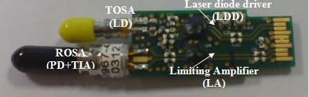
The module includes TOSA, ROSA and PCBA, in which only TOSA is metal and is connected to the shell.
To replace the TOSA; then to observe whether it is short circuit. If it is short circuit, the PCBA is bad, or the TOSA is bad. In this case, we should replace the TOSA or scrap the PCBA.
Reason and Maintenance methods of common problem of optical module externally
1. Power light does not light.
Reason: Power supply fault.
Maintenance method: Replace the power supply.
2. Link lights are not lit.
Failure may be as follows:
(A) Check whether the fiber lines circuit breakers
(B) Check whether the fiber line loss is too great, over equipment reception range
(C) Check whether the optical interfaces are connected properly, local TX and RX connections from afar, TX and RX connections of the local in the distance.
(D) Check whether the optical fiber connector intact, insert a device interface, jumper type matches the device interfaces, device type matches the fiber, equipment transfer length matches the distance.
3. The circuit Link light does not light.
Failure may be as follows:
(A) Check that the network cable is the circuit breaker.
(B) Check the connection matches the type: devices such as network cards and routers use a crossover cable, Switches, hubs and other equipment using the straight line.
(C) Check whether the equipment transfer rate matches.
4. Serious network packet
Possible fault is as follows:
(1) The transceiver's power port and the network device interface or device interface duplex mode don’t match on both ends.
(2) RJ-45 head and twisted issues, testing
(3) The fiber connectivity issues, device interface jumper are alignment, pigtail coupler and jumper match the types, and so on.
5. Fiber optic transceiver ends cannot communicate.
Possible fault is as follows:
(1) Optical fiber connected backwards, TX and RX fiber swap
(2) RJ45 interface and the external device is not connected properly (note the pass-through and splicing).
Optical fiber interface (ceramic ferrule) do not match, this failure is mainly reflected in the 100M belt on optical transceivers for mutual control function, such as APC ferrule fiber received PC ferrule on the transceiver will not communicate correctly, but does not affect mutual control of non-optical transceiver.
6. The communication after a period of time to panic, not communication, after the resumption of normal.
This is generally caused by a switch, switch all the received data length for CRC error detection and verification, checks out the package with errors will be discarded, the correct package will be forwarded.
But there is some error in the package of this process in both the length of CRC error detection and checksum is not detected, this package will not be sent out during the forwarding process, will not be discarded.
They will be stacked in a dynamic cache (buffer), never sent, accumulate in wait until the buffer is full, switch to panic would be caused.
Because the transceiver or switch traffic back to normal, so the user usually considered problems of the transceiver.
7. If transceiver test methods have problems, follow these methods for testing in order to find the cause of failure.
A) Proximal test:
Computers at both ends on the PING, PING Tong prove that fiber optic transceivers are not problems. Proximal tests cannot be judged as media of communication failures.
B) Remote test:
Computers at both ends on the PING, PING general clauses must check whether the optical connection of normal and fiber optic transceivers transmit and receive power is within the allowed range. If they can prove the General PING road connectivity, to check malfunction switch the problem.
C) Remote test to determine points of failure:
Switch end, ends the PING, if no fault can be judged as another switch fault.
8. Others
(1) May be the optical attenuation is too large, available optical power for optical power meters measure the receiving end, if in the vicinity of receiver sensitivity range, 1-2dB within the basic judgment of light path failures
(2) The switch faults may be connected to the transceiver, switch to PC switches, namely two transceivers and direct connection to the PC, PING at both ends, as does not appear broken when basic judgment as switch failures
(3) Potential as transceiver failed, then the transceiver at both ends PC (via switches), ends after the PING is no problem, from one end to the other end to send a large file (100M) or more, watch it speed, such as slow speed (200M following file transfer for more than 15 minutes), basic judgment for the sending and receiving faults.
Important reason for the optical module functional failure
- Optical Interface is polluted and damaged.
The pollution and damage of the optical interface causes the optical link loss become large, resulting in the optical link fails.
Reason as follows:
- The interface is explored in the environment so that the dust pollutes the interface.
- The fiber connector which is used has been polluted so that it causes the secondary pollution.
- Improper use of the interface of the optical connector with pigtail.
- The use of poor quality fiber optic connectors.
- ESDM damage
ESD is the abbreviation of Electro Static Discharge. ESD can produce tens of kv/m of electromagnetic pulse and even more.
Static electricity will absorb dust, changing impedance line and affecting the life and function of the product.
The heat produced by instantaneous electric field or current of the ESD will damage components. They may work in short-term, but their life is still affected.
The heat even damages the insulation or conductor of components, which will makes the components don’t work (or completely destroyed).
ESD is inevitable. In addition to improving the ESD immunity of electronic components, the more importance is to use the electronic components properly.
ESD damage causing factors are as follow:
- Dry environment which easily produce the ESD.
- Abnormal operation. For example, operate the non-hot-pluggable optical modules with power; directly touch the static-sensitive pin [t2] of the optical module by hand without ESD protection; there is not anti-static packaging during the transport and storage process.
- Equipment is not grounded or poorly grounded.
You May Want to Know: