-

- Sopto Home
-

- Special Topic
-
- PCI-E Card Knowledge
-
- Selecting the Optimum PCI Express Clock Source

PCI-E Card Knowledge
- Info about Network Interface Card Teaming
- How to Setup a Server with Multiple Network Interface Adapters?
- How to Reconnect an Internet Network Adapter for an Acer Aspire?
- 9 Things to Do When Your Internal Network Card Stops Working
- Ethernet Standards NIC for Home Networking
- What Is a Network Interface Adapter?
- How to Configure a Network Interface Card in Linux?
- How should Configure Your NIC for ISA and TMG?
- Recommended Network Card Configuration for Forefront UAG Servers
SOPTO Special Topic
Certificate

Guarantee
Except products belongs to Bargain Shop section, all products are warranted by SOPTO only to purchasers for resale or for use in business or original equipment manufacturer, against defects in workmanship or materials under normal use (consumables, normal tear and wear excluded) for one year after date of purchase from SOPTO, unless otherwise stated...
Return Policies
Defective products will be accepted for exchange, at our discretion, within 14 days from receipt. Buyer might be requested to return the defective products to SOPTO for verification or authorized service location, as SOPTO designated, shipping costs prepaid. .....
Applications
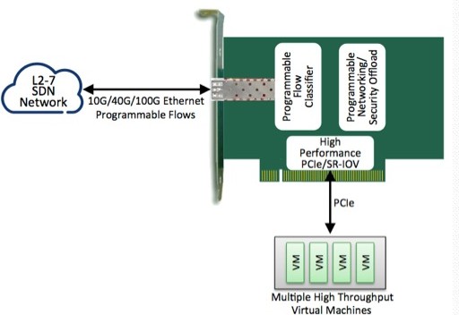
PCI-E NIC Cards provide redundant connectivity to ensure an uninterrupted network connection.
PCI-E NIC Cards are ideal for VM environments with multiple operating systems, requiring shared or dedicated NICs.
They are specially designed for desktop PC clients, servers, and workstations with few PCI Express slots available.
SNS Page


SOPTO Products
- Fiber Optic Transceiver Module
- High Speed Cable
- Fiber Optical Cable
- Fiber Optical Patch Cords
- Splitter CWDM DWDM
- PON Solution
- FTTH Box ODF Closure
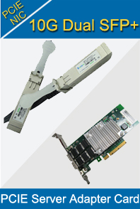
- PCI-E Network Card
- Network Cables
- Fiber Optical Adapter
- Fiber Optical Attenuator
- Fiber Media Converter
- PDH Multiplexers
- Protocol Converter
- Digital Video Multiplexer
- Fiber Optical Tools
- Compatible
Related Products
Performance Feature
PCI-E Card Knowledge
Recommended
Selecting the Optimum PCI Express Clock Source
PCI Express (PCIe) is a serial point - to - point interconnect standard developed by the Peripheral Component Interconnect Special Interest Group (PCI- SIG). Although originally designed for desktop personal computers, the PCIe standard has been widely adopted in a broad range of applications including blade servers, storage, embedded computing, and networking and communications. Not only is the PCIe interface supported by a wide base of commercially available devices, it is also becoming more readily available in FPGAs and SoCs, providing designers with flexible solutions for transferring data within their systems. One of the key advantages of using PCIe is its scalable data bandwidth and flexible clocking solutions.
Let’s explore some of the standard clocking architectures for PCIe and consider their benefits for typical system applications.
The PCIe Link
Before considering clocking architectures, let’s examine a PCIe data link. It consists of one or more lanes that provide a transmit (Tx) and receive (Rx) differential pair. Figure 2 shows two devices that need to transfer data. One of the key advantages of PCIe is its bandwidth scalability enabling up to 32 lanes to be configured on a single link. With the recent introduction of PCIe 3.0, each lane can accommodate 8 Gbits per second (Gbps) per direction for a maximum data throughput of 64Gbps of data transfer.
Applications that need less data bandwidth can simply be configured with fewer lanes. Previous PCIe 1.1 and 2.1 standards offer 2.5 Gbps and 5.0Gbps per lane respectively. Choosing a PCIe standard with higher data rates ultimately means using less lanes or connection wires between devices, but it also places additional requirements on the clocking performance. We will examine these requirements in the following sections.
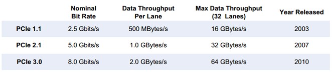
Figure1. Different PCIe Version
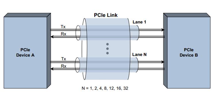
Figure2. PCI Express Link
PCIe Applications
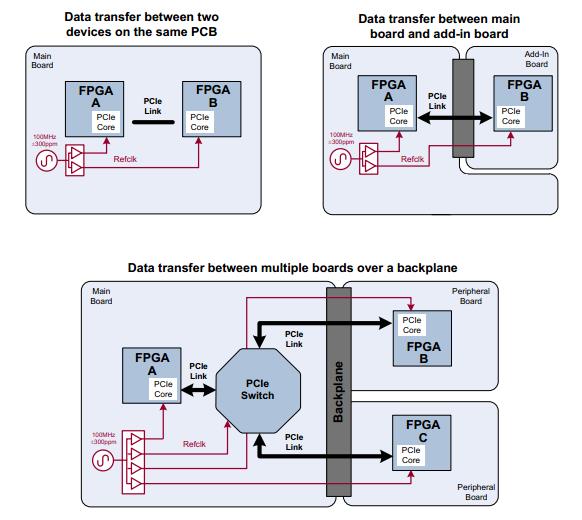
Figure3. System Applications of PCIe Interconnects
PCIe Clocking Architectures
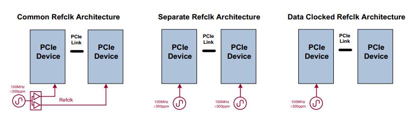
Figure4. PCIe Clocking Architectures
An alternative is to use the Separate Refclk architecture where a different clock source is used at each end of the PCIe link. Both clock sources can still have a frequency accuracy of ±300 ppm since the PCI Express standard allows for a total frequency deviation of 600 ppm between the transmitter and receiver, but it leaves no extra frequency margin for enabling spread spectrum clocking.
Figure5. PCIe Clocking Architectures
Spread Spectrum Clocking (SSC)