-

- Sopto Home
-

- Special Topic
-
- Twinax Cable Knowledge
-
- Typical QSFP+ Connector Inner Structure
Twinax Cable Knowledge
- Cable Labeling as Part of Data Center Management
- How to Correctly Run cables On Servers in a Data Center?
- 4 Realities You Should Consider 10G Ethernet for Your Business
- Is it finally the end of copper?
- Why We Need Both 40G and 100G Ethernet Cable?
- What is Twisted Pair Cable?
- Benefits of Twisted Pair Cable Construction
- Why Copper Is Used in Cables?
- A Brief Look at Ethernet Cable Construction
SOPTO Special Topic
Certificate


Guarantee
Except products belongs to Bargain Shop section, all products are warranted by SOPTO only to purchasers for resale or for use in business or original equipment manufacturer, against defects in workmanship or materials under normal use (consumables, normal tear and wear excluded) for one year after date of purchase from SOPTO, unless otherwise stated...
Return Policies
Defective products will be accepted for exchange, at our discretion, within 14 days from receipt. Buyer might be requested to return the defective products to SOPTO for verification or authorized service location, as SOPTO designated, shipping costs prepaid. .....
Applications
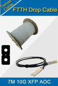
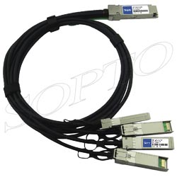
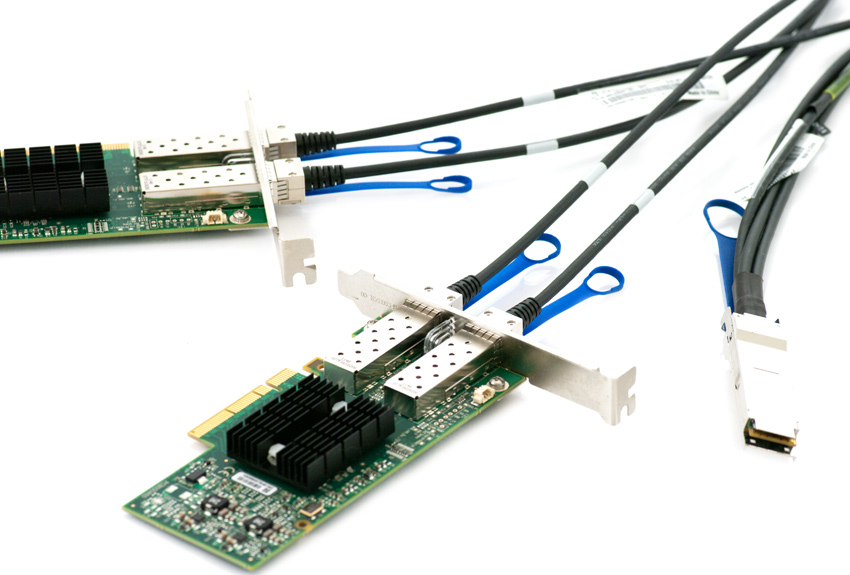 Twinax Cables are mainly used with PCI or PCI-E Card for the short distance interconnection in the server room.
SNS Page


SOPTO Products
- Fiber Optic Transceiver Module
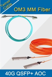
- High Speed Cable
- Fiber Optical Cable
- Fiber Optical Patch Cords
- Splitter CWDM DWDM
- PON Solution
- FTTH Box ODF Closure
- PCI-E Network Card
- Network Cables
- Fiber Optical Adapter
- Fiber Optical Attenuator
- Fiber Media Converter
- PDH Multiplexers
- Protocol Converter
- Digital Video Multiplexer
- Fiber Optical Tools
- Compatible
Related Products
Performance Feature
Stable Transmission Speed
Reliable Transmission
Various Length Selection
Wider Operating Temperature
Good for HPC
Good for Data Center
Twinax Cable Knowledge
Recommended
Typical QSFP+ Connector Inner Structure
Along with the production about server virtualization and additionally impair computing and the phenomena about mobile phone network integration. Accelerate and additionally more significant economic dependence on the knowledge coronary heart mobile phone network is normally higher and higher.
QSFP+ SR4 module is ascribed to all the high-density 10G and additionally 40G Ethernet aggregation, featuring improved suppleness to get in touch varied levels’ changes and also lessen all the lag time. This kind of QSFP+ SR4 fiber optic transceiver equally makes more significant bond occurrence on the smaller vitality use of any channel.
A typical QSFP+ connector attached to the ends of an AOC cable is shown in Figure 1.
Figure 1

Typical QSFP+ Connector
The QSFP+ module assembly consists of an optical ribbon fiber cable attached to the PN1000001 Si CMOS photonics chip, which is mounted on a printed circuit board (PCB) and placed within an electromagnetic interference (EMI) shielded metal housing, shown in Figure 2. The PN1000001 Si CMOS photonics chip is wire bonded directly to the PCB as shown in Figure 3.
Figure 2

PCB of QSFP+ Module Assembly
Figure 3

PN1000001 Si CMOS Photonics Die Wire bonded to the PCB Plan View
The Si CMOS photonics chip was removed from the PCB and the gel over the chip carefully removed in our lab to expose the structure of the module featuring the Si CMOS photonics die. Figure 4 and Figure 5 are tilt and cross-sectional views, respectively, of the module featuring a laser module and optical fiber assembly attached to the top surface of the PN1000001 Si CMOS photonics die. The Si CMOS photonics die is attached to a metal support.
Figure 4

Si CMOS Photonics Die Module – Tilt View
Figure 5

Si CMOS Photonics Die module Optical Cross Section
Figure 6 is a detailed cross-sectional SEM image showing the coupling between the optical fiber and Si CMOS chip. The fiber assembly is epoxied to the top of the Si CMOS chip such that each fiber is centered over a grating coupler. The fiber core is located in the middle of the fiber cladding and is not visible in this cross-sectional image.
Figure 6

Optical Fiber to Si Chip Coupling SEM Cross Section
Figure 7 and Figure 8 show plan and side-view X-ray images, respectively, of the laser module attached to the PN1000001 Si CMOS photonics die. The laser module is similar to laser modules used in typical fiber-to-home applications, but modified to bounce the light originating from the side of the laser die into the Si photonics chip. The laser module consists of a laser die, ball lens, and isolator, all aligned and positioned over a micro-machined Si optical bench and covered with a Si cap that is etched to form a cavity over the laser module elements. The underside part of the cap is coated with a reflector, which bounces light from the laser into the Si photonics die.
Figure 7

Laser module – plan-view X-ray
Figure 8

Laser module – side-view X-ray
A die photograph of the PN1000001 Si CMOS photonics die extracted from the module is shown in Figure 9. The transceiver die uses four transmit (TX) and four receive (RX) channels, a digital core, and eight fiber array I/Os. The die also features a channel transmit section in the lower half of the die and a four-channel receive section in the upper half of the die.
Figure 9

PN1000001 Die Photograph
The transmit (TX) channels feature light from the laser module that is coupled into the chip near the lower left edge of the chip, using single polarization grating couplers (SPGC). The coupled light is transported using single mode (SMW) and multiple mode (MMW) waveguides, built into the SOI layer of the chip, into the two arms of a segmented high-speed Mach-Zehnder modulator interferometer (MZI) chain placed near the lower left quarter of the die.
Electrical signals coupled into the lower left edge of the chip modulate the optical signal in the MZI arms, by biasing the built-in reverse biased PN junction diode of the MZI, and inducing a phase change between the optical signals in the two arms of the MZI, which results in an amplitude modulated optical signal. Waveguides carry the modulated light from MZI to four grating couplers (SPGC) to couple light from the four TX channels to four optical fibers that carry the light out of the chip. These optical fibers are in the lower four fibers of the eight fibers connected at the right half of the die. On the way towards the output, the optical signal is tapped and monitored.
The receive (RX) channels placed under the upper four fibers of the die couple light into the chip using polarization splitting couplers (PSGC). Four PSGC structures are beneath the four upper optical fibers connected at the right edge of the die. The light coupled into the receive channels travels using SMW and MMW waveguides, from the right to the left edge of the die, to reach the front end of the receiver channels. The front ends of the four channels of the receiver placed near the upper left quarter of the device feature a Ge PIN photodetector, which detects the optical light and converts to an electrical signal. The electrical signal from each RX channel is amplified further by multistage transimpedence and limiting amplifiers.
For more info, please browse our website or contact a Sopto representative by calling 86-755-36946668, or by sending an email to info@sopto.com.