
- Sopto Home
-

- 40G 850nm 150m QSFP+ SR4 Fiber Optic Transceiver Module SPT-QSFP-SR4
- Fiber Optic Transceiver Module
- High Speed Cable
- Fiber Optical Cable
- Fiber Optical Patch Cords
- Splitter CWDM DWDM
- PON Solution
- FTTH Box ODF Closure
- PCI-E Network Card
- Network Cables
- Fiber Optical Adapter
- Fiber Optical Attenuator
- Fiber Media Converter
- PDH Multiplexers
- Protocol Converter
- Digital Video Multiplexer
- Fiber Optical Tools
- Compatible
40G 850nm 150m QSFP+ SR4 Fiber Optic Transceiver Module SPT-QSFP-SR4

SPT-QSFP+-SR4
QSFP+ SR4 Transceiver
Features
Four-channel full-duplex transceiver modules
Transmission data rate up to 10.3Gbit/s per channel
4 channels 850nm VCSEL array
4 channels PIN photo detector array
Low power consumption <1.5W
Housing isolated from connector ground
Operating case temperature 0°C to +70°C
3.3V power supply voltage
RoHS 6 compliant
Hot Pluggable QSFP form factor
Maximum link length of 100m on OM3 Multimode Fiber (MMF)and 150m on OM4 MMF
Single MPO connector receptacle
Built-in digital diagnostic functions
Applications
40GBASE-SR4 40G Ethernet
Dotcom/Telecom switch & router connections
Data Aggregation and Backplane Applications
Proprietary Protocol and Density Applications
Description
SPT-QSFP-SR4 is a Four-Channel, Pluggable, Parallel, and Fiber-Optic QSFP+ Transceiver for 40 Gigabit Ethernet Applications. This transceiver is a high performance module for short-range multi-lane data communication and interconnects applications. It integrates four data lanes in each direction with 40 Gbps bandwidth. Each lane can operate at 10.3125 Gbps up to 100 m using OM3 fiber or 150 m using OM4 fiber. These modules are designed to operate over multimode fiber systems using a nominal wavelength of 850nm. The electrical interface uses a 38 contact edge type connector. The optical interface uses a 12 fiber MTP (MPO) connector. This module incorporates Technologies proven circuit and VCSEL technology to provide reliable long life, high performance, and consistent service.
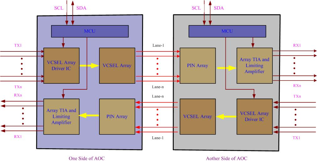
Figure1. Module Block Diagram
SPT-QSFP+ SR4 are one kind of parallel transceiver. VCSEL and PIN array package is key technique, through I2C system can contact with module
Absolute Maximum Ratings
|
Parameter |
Symbol |
Min |
Max |
Unit |
|
Supply Voltage |
Vcc |
-0.3 |
3.6 |
V |
|
Input Voltage |
Vin |
-0.3 |
Vcc+0.3 |
V |
|
Storage Temperature |
Tst |
-20 |
85 |
ºC |
|
Case Operating Temperature |
Top |
0 |
70 |
ºC |
|
Case Operating Temperature |
Rh |
5 |
95 |
% |
Recommended Operating Conditions
|
Parameter |
Symbol |
Min |
Typical |
Max |
Unit |
|
Supply Voltage |
Vcc |
313. |
3.3 |
3.47 |
V |
|
Operating Case temperature |
Tca |
0 |
|
70 |
ºC |
|
Data Rate Per Lane |
fd |
2.5 |
|
10.3 |
Gbps |
|
Humidity |
Rh |
5 |
|
85 |
% |
|
Power Dissipation |
Pm |
|
|
1.5 |
W |
|
Fiber Bend Radius |
Rb |
3 |
|
|
cm |
Specifications
|
Parameter |
Symbol |
Min |
Typical |
Max |
Unit |
|
Differential input impedance |
Zin |
90 |
100 |
110 |
Ohm |
|
Differential Output impedance |
Zout |
90 |
100 |
110 |
Ohm |
|
Differential input voltage amplitude a Amplitude |
ΔVin |
300 |
|
1100 |
mVp-p |
|
Differential output voltage a mplitude |
ΔVout |
500 |
|
800 |
mVp-p |
|
Skew |
Sw |
|
|
300 |
ps |
|
Bit Error Rate |
BR |
|
|
E-12 |
|
|
Input Logic Level High |
VIH |
2.0 |
|
VCC |
V |
|
Input Logic Level Low |
VOL |
0 |
|
0.8 |
V |
|
Output Logic Level High |
VOH |
VCC-0.5 |
|
VCC |
V |
|
Output Logic Level Low |
VOL |
0 |
|
0.4 |
V |
Note:
BER=10 -12; PRBS 2 31-1@10.3125Gbps.
2. Differential input voltage amplitude is measured between TxNp and TxNn.
3. Differential output voltage amplitude is measured between RxNp and RxNn.
Pin Descriptions
|
Pin |
Logic |
Symbol |
Name/Description |
Ref |
|
1 |
|
GND |
Module Ground |
1 |
|
2 |
CML-I |
Tx2- |
Transmitter inverted data input |
|
|
3 |
CML-I |
Tx2- |
Transmitter non-inverted data input |
|
|
4 |
|
GND |
Module Ground interface |
2 |
|
5 |
CML-I |
Tx4- |
Transmitter inverted data input |
|
|
6 |
CML-I |
Tx4- |
Transmitter non-inverted data input |
|
|
7 |
|
GND |
Module Ground |
1 |
|
8 |
LVTTL-I |
MODSEIL |
Module Select |
|
|
9 |
LVTTL-I |
ResetL |
Module Reset |
|
|
10 |
|
VCCRx |
+3.3v Receiver Power Supply |
2 |
|
11 |
LVCMOS-I |
SCL |
2-wire Serial interface clock |
2 |
|
12 |
LVCMOS-I/O |
SDAs |
2-wire Serial interface data |
2 |
|
13 |
|
GND |
Module Ground |
2 |
|
14 |
CML-O |
RX3+ |
Receiver non-inverted data output |
2 |
|
15 |
CML-O |
RX3+ |
Receiver inverted data output |
1 |
|
16 |
|
GND |
Module Ground |
1 |
|
17 |
CML-O |
RX1- |
Receiver non-inverted data output |
|
|
18 |
CML-O |
RX1+ |
Receiver inverted data output |
|
|
19 |
|
GND |
Module Ground |
1 |
|
20 |
|
GND |
Module Ground |
|
|
21 |
CML-O |
RX2 |
Receiver inverted data output |
|
|
22 |
CML-O |
RX2 |
Receiver non-inverted data output |
|
|
23 |
|
GND |
Module Ground |
1 |
|
24 |
CML-O |
RX4 |
Receiver inverted data output |
|
|
25 |
CML-O |
RX4- |
Receiver non-inverted data output |
|
|
26 |
|
GND |
Module Ground |
1 |
|
27 |
LVTTL-O |
Mod PrsL |
Module Present, internal pulled down to GND |
|
|
28 |
LVTTL-O |
IntL- |
Interrupt output, shouldbe pulled up on host board |
2 |
|
29 |
|
VCCTx |
+3.3v Transmitter Power Supply |
|
|
30 |
|
VCC1 |
+3.3v Power Supply |
|
|
31 |
LVTTL-I |
LP Mode |
Low Power Mode |
2 |
|
32 |
|
GND |
Module Ground |
1 |
|
33 |
CML-I |
Tx3+ |
Transmitter non-inverted data input |
|
|
34 |
CML-I |
Tx3- |
Transmitter inverted data input |
|
|
35 |
|
GND |
Module Ground |
1 |
|
36 |
CML-I |
Tx1+ |
Transmitter non-inverted data input |
|
|
37 |
CML-I |
Tx1- |
Transmitter inverted data input |
|
|
38 |
|
GND |
Module Ground |
1 |
Notes:
1. Module circuit ground is isolated from module chassis ground within the module.
2. Open collector; should be pulled up with 4.7k – 10k ohms on host board to a voltage between 3.15Vand 3.6V.
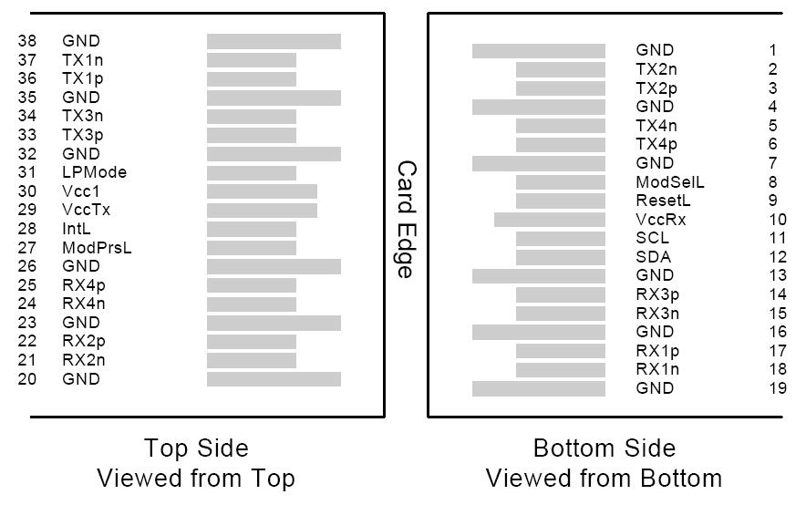
Figure2. Electrical Pin-out Details
Mod SelL Pin
The mod Sell is an input pin. When held low by the host, the module responds to 2-wire serial communication commands. The Modell allows the use of multiple QSFP modules on a single 2-wire interface bus. When the mod Sell is “High”, the module will not respond to any 2-wire interface communication from the host. mod Sell has an internal pull-up in the module.
ResetL Pin
Reset. LPMode_Reset has an internal pull-up in the module. A low level on the Resettle pin for longer than the Minimum pulse length (t_Reset_init) initiates a complete module reset, returning all user module settings totheir default state. Module Reset Assert Time (t_init) starts on the rising edge after the low level on the ResetL pin is released. During the execution of a reset (t_init) the host shall disregard all status bits until the module indicates a completion of the reset interrupt. The module indicates this by posting an IntL signal withthe Data_Not_Ready bit negated. Note that on power up (including hot insertion) the module will post this completion of reset interrupt without requiring a reset.
LPMode Pin
SPT-QSFP+ SR4 operate in the low power mode (less than 1.5 W power consumption)
This pin active high will decrease power consumption to less than 1W.
ModPrsL Pin
ModPrsL is pulled up to Vcc on the host board and grounded in the module. The ModPrsL is asserted “Low “when the module is inserted and deserted “High” when the module is physically absent from the host connector.
IntL Pin
IntL is an output pin. When “Low”, it indicates a possible module operational fault or a status critical to the host system. The host identifies the source of the interrupt by using the 2-wire serial interface. The Intel pin is an open collector output and must be pulled up to Vcc on the host board
Power Supply Filtering
The host board should use the power supply filtering shown in Figure3.
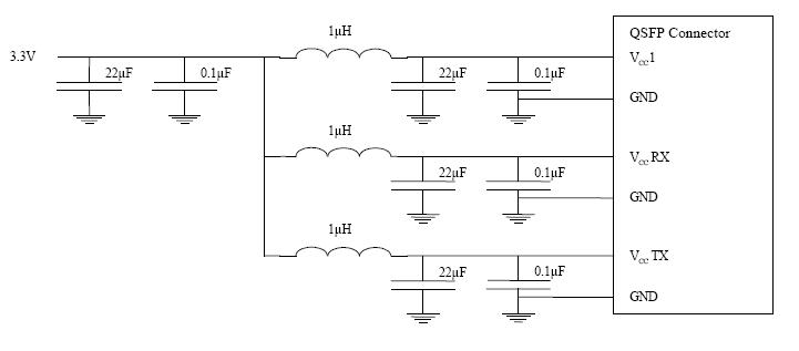
Figure3. Host Board Power Supply Filtering
DIAGNOSTIC MONITORING INTERFACE
Digital diagnostics monitoring function is available on all SOPTO SPT-QSFP-SR4. A 2-wire serial interface provides user to contact with module.
The structure of the memory is shown in Figure 4. The memory space is arranged into a lower, single page, address space of 128 bytes and multiple upper address space pages. This structure permits timely access to addresses in the lower page, such as Interrupt Flags and Monitors. Less time critical time entries, such as serial ID information and threshold settings, are available with the Page Select function.
The interface address used is A0xh and is mainly used for time critical data like interrupt handling in order to enable a one-time-read for all data related to an interrupt situation. After an interrupt, IntL, has been asserted, the host can read out the flag field to determine the affected channel and type of flag.
.jpg)
Figure4. QSFP Memory Map
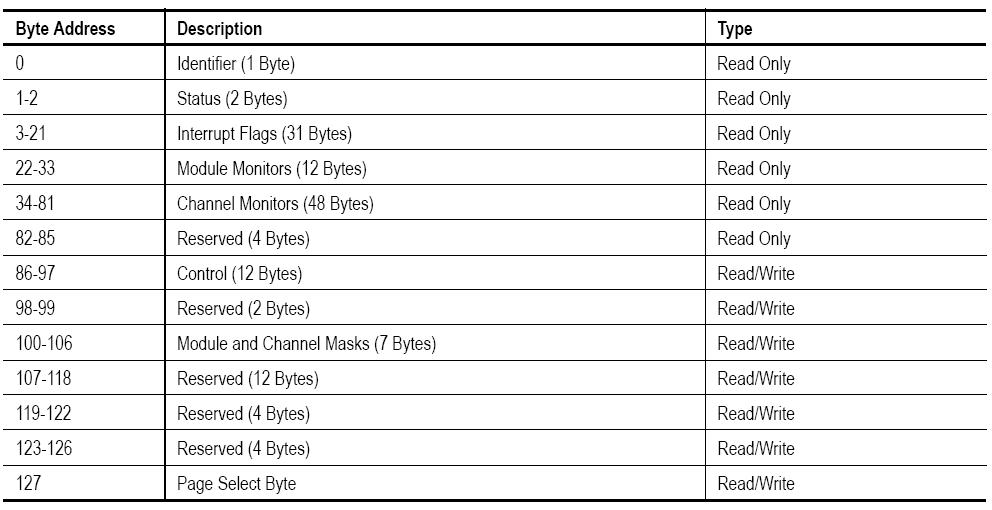
Figure5. Low Memory Map
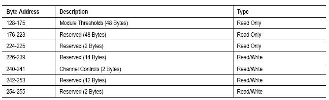
Figure6. Page 03 Memory Map
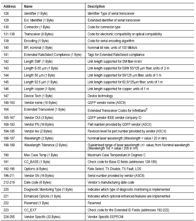
Figure7. Page 00 Memory Map
Timing for Soft Control and Status Functions
|
Parameter |
Symbol |
Max |
Unit |
Conditions |
|
Initialization Time |
t_init |
2000 |
ms |
Time from power on1, hot plug or rising edge of Reset until the module is fully functional2 |
|
ResetInit Assert Time |
t_reset_init |
2 |
μs |
A Reset is generated by a low level longer than the minimum reset pulse time present on the Reset pin. |
|
Serial Bus Hardware Ready Time |
t_serial |
2000 |
ms |
Time from power on 1 until module responds to data transmission over the 2-wire serial bus |
|
Monitor Data Ready Time |
t_data |
2000 |
ms |
Time from power on 1 to data no tready, bit 0 of Byte 2, deserted and Intel asserted |
|
Reset Assert Time |
t_reset |
2000 |
ms |
Time from rising edge on the Reset pin until the module is fully functional 2 |
|
LP Mode Assert Time |
ton_LPMode |
100 |
μs |
Time from assertion of LP Mode (Vin:LPMode=Vih) until module power consumption enters lower Power Level |
|
IntL Assert Time |
ton_IntL |
200 |
ms |
Time from occurrence of condition triggering Intel until Vout:IntL=Vol |
|
IntL Deassert Time |
toff_IntL |
500 |
μs |
Time from clear on read 3 operation of associated flag until Vout:IntL=Voh. This includes dessert times for Rx LOS, TX Fault and other flag bits. |
|
Rx LOS Assert Time |
ton_los |
100 |
ms |
Time from Rx LOS state to Rx LOS bit set and Intel asserted |
|
Tx Fault Assert Time |
ton_Tx fault |
200 |
ms |
Time from TX Fault state to TX Fault bit setand Intel asserted |
|
Flag Assert Time |
ton_flag |
200 |
ms |
Time from occurrence of condition triggering flag to associated flag bit setand Intel asserted |
|
Mask Assert Time |
ton_mask |
100 |
ms |
Time from mask bit set 4 until associated Intel assertion is inhibited |
|
Mask Deassert Time |
toff_mask |
100 |
ms |
Time from mask bit cleared4 until associated Install operation resumes |
|
ModSelL Assert Time |
ton_ModSelL |
100 |
μs |
Time from assertion of Modell until module responds to data transmission over the 2-wire serial bus |
|
ModSelL Deassert Time |
toff_ModSelL |
100 |
μs |
Time from desertion of Modell until the module does not respond to data transmission over the 2-wire serial bus |
|
Power_over-ride or Power-set Assert Time |
ton_P down |
100 |
ms |
Time from desertion of Modell until the module does not respond to data transmission over the 2-wire serial bus |
|
Power_over-ride or Power-set Dessert Time |
toff_P down |
300 |
ms |
Time from P_Down bit cleared 4 until the module is fully functional 3 |
Notes:
1. Power on is defined as the instant when supply voltages reach and remain at or above the minimum specified value.
2. Fully functional is defined as Intel asserted due to data not ready bit, bit 0 byte 2 deserted.
3. Measured from falling clock edge after stop bit of read transaction.
4. Measured from falling clock edge after stop bit of write transaction.
Mechanical Dimensions
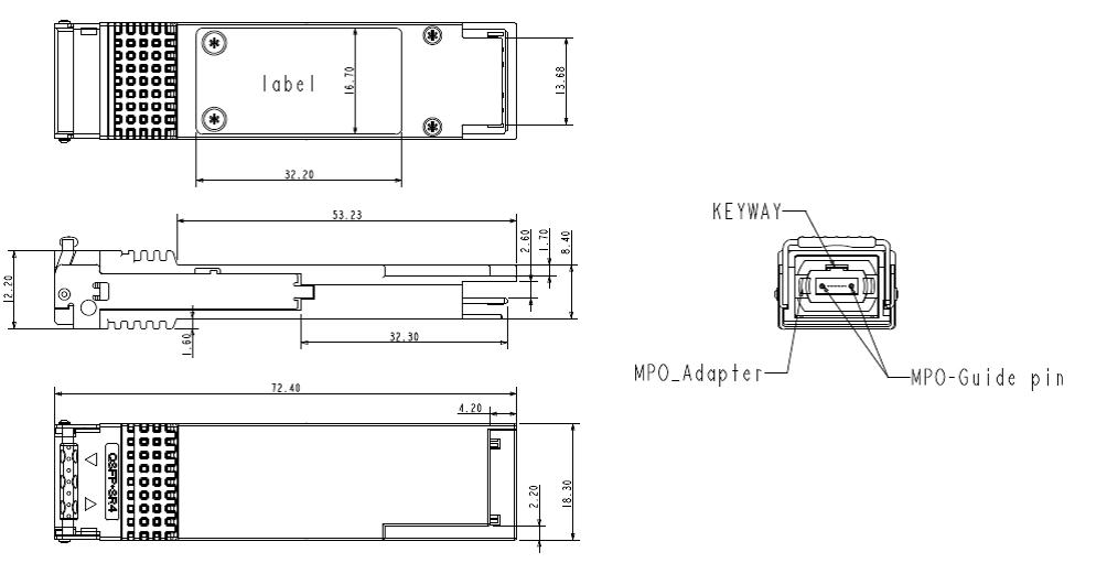
Figure8. Timing Specifications
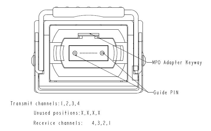
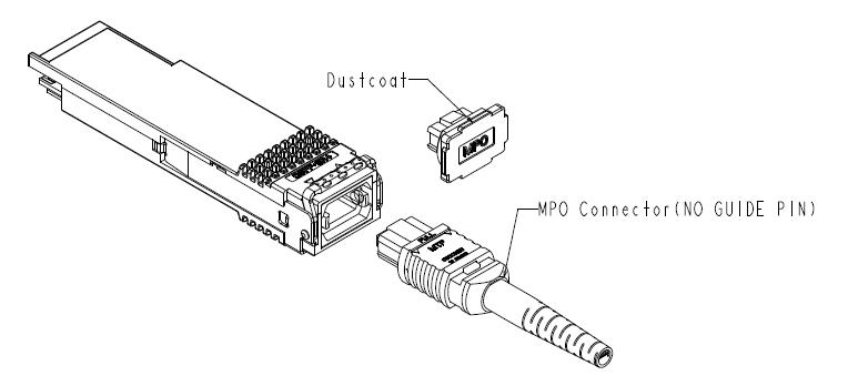
Figure9. Mechanical Specifications
Ordering information
|
Part Number |
Product Description |
|
SPT-QSFP-SR4 |
XXX=different cable lengths |
|
XX(X) |
Length |
|
03 |
003=3m |
|
05 |
005=5m |
|
10 |
010=10m |
|
20 |
020=20m |
|
50 |
050=50m |
|
100 |
100=100m |
E-mail:sales@sopto.com