
- Sopto Home
-

- SPT-QSFP+-IR4 40Gb/s QSFP+ IR4 Optical Transceiver
- Fiber Optic Transceiver Module
- High Speed Cable
- Fiber Optical Cable
- Fiber Optical Patch Cords
- Splitter CWDM DWDM
- PON Solution
- FTTH Box ODF Closure
- PCI-E Network Card
- Network Cables
- Fiber Optical Adapter
- Fiber Optical Attenuator
- Fiber Media Converter
- PDH Multiplexers
- Protocol Converter
- Digital Video Multiplexer
- Fiber Optical Tools
- Compatible
SPT-QSFP+-IR4 40Gb/s QSFP+ IR4 Optical Transceiver

SPT-QSFP+-IR4
40Gb/s QSFP+ IR4 Optical Transceiver
Features
- 4 CWDM lanes MUX/DEMUX design
- Up to 12.5Gbps data rate per wavelength
- QSFP+ MSA compliant
- IEEE 802.3ba Electrical Interface
- Up to 2km transmission
- Optical link budget: 9.5dB
- Operating case temperature: 0~70C
- Maximum 3.5W operation power
- SMF LC duplex connector
- RoHS compliant
Applications
- 40G Campus Link
- Infiniband interconnects
- 40G Telecom connections
- Data Center Interconnect
General Description
This product is a transceiver module designed for 2m-2km optical communication applications. The design is reference to 40GBASE-IR4 of the IEEE P802.3ba standard. The module converts 4 inputs channels (ch) of 10Gb/s electrical data to 4 CWDM optical signals, and multiplexes them into a single channel for 40Gb/s optical transmission. Reversely, on the receiver side, the module optically de-multiplexes a 40Gb/s input into 4 CWDM channels signals, and converts them to 4 channel output electrical data.
The central wavelengths of the 4 CWDM channels are 1271, 1291, 1311 and 1331 nm as members of the CWDM wavelength grid defined in ITU-T G694.2. It contains a duplex LC connector for the optical interface and a 148-pin connector for the electrical interface. To minimize the optical dispersion in the long-haul system, single-mode fiber (SMF) has to be applied in this module.
The product is designed with form factor, optical/electrical connection and digital diagnostic interface according to the QSFP+ Multi-Source Agreement (MSA). It has been designed to meet the harshest external operating conditions including temperature, humidity and EMI interference.
Functional Description
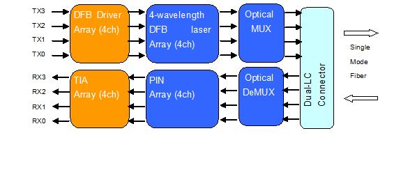
- This product converts the 4-channel 10Gb/s electrical input data into CWDM optical signals (light), by a driven 4-wavelength Distributed Feedback Laser (DFB) array. The light is combined by the MUX parts as a 40Gb/s data, propagating out of the transmitter module from the SMF. The receiver module accepts the 40Gb/s CWDM optical signals input, and de-multiplexes it into 4 individual 10Gb/s channels with different wavelength. Each wavelength light is collected by a discrete photo diode, and then outputted as electric data after amplified by a TIA. Figure 1 shows the functional block diagram of this product.
- A single +3.3V power supply is required to power up this product. Both power supply pins VccTx and VccRx are internally connected and should be applied concurrently. As per MSA specifications the module offers 7 low speed hardware control pins (including the 2-wire serial interface): ModSelL, SCL, SDA, ResetL, LPMode, ModPrsL and IntL.
- Module Select (ModSelL) is an input pin. When held low by the host, this product responds to 2-wire serial communication commands. The ModSelL allows the use of this product on a single 2-wire interface bus – individual ModSelL lines must be used.
- Serial Clock (SCL) and Serial Data (SDA) are required for the 2-wire serial bus communication interface and enable the host to access the QSFP+ memory map.
- The ResetL pin enables a complete reset, returning the settings to their default state, when a low level on the ResetL pin is held for longer than the minimum pulse length. During the execution of a reset the host shall disregard all status bits until it indicates a completion of the reset interrupt. The product indicates this by posting an IntL (Interrupt) signal with the Data_Not_Ready bit negated in the memory map. Note that on power up (including hot insertion) the module should post this completion of reset interrupt without requiring a reset.
- Low Power Mode (LPMode) pin is used to set the maximum power consumption for the product in order to protect hosts that are not capable of cooling higher power modules, should such modules be accidentally inserted.
- Module Present (ModPrsL) is a signal local to the host board which, in the absence of a product, is normally pulled up to the host Vcc. When the product is inserted into the connector, it completes the path to ground though a resistor on the host board and asserts the signal. ModPrsL then indicates its present by setting ModPrsL to a “Low” state.
- Interrupt (IntL) is an output pin. “Low” indicates a possible operational fault or a status critical to the host system. The host identifies the source of the interrupt using the 2-wire serial interface. The IntL pin is an open collector output and must be pulled to the Host Vcc voltage on the Host board.
Transceiver Block Diagra
Figure 1: 40Gb/s QSFP+ GR4 Transceiver Block Diagram
Pin Assignment and Pin Description
Figure 2: MSA compliant Connector
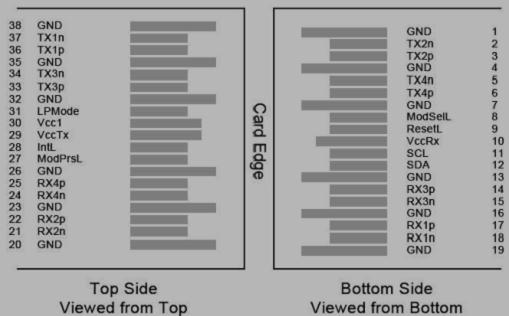
Pin Definitions
|
PIN |
Logic |
Symbol |
Name/ Description |
Note |
|
1 |
|
GND |
Ground |
1 |
|
2 |
CML-I |
Tx2n |
Transmitter Inverted Data Input |
|
|
3 |
CML-I |
Tx2p |
Transmitter Non-Inverted Data output |
|
|
4 |
|
GND |
Ground |
1 |
|
5 |
CML-I |
Tx4n |
Transmitter Inverted Dat aInput |
|
|
6 |
CML-I |
Tx4p |
Transmitter Non- Inverted Data output |
|
|
7 |
|
GND |
Ground |
1 |
|
8 |
LVTLL-I |
ModSelL |
Module Select |
|
|
9 |
LVTLL-I |
ResetL |
Module Reset |
|
|
10 |
|
VccRx |
+3.3V Power Supply Reciver |
2 |
|
11 |
LVCMOS-I/O |
SCL |
2-Wire Serial Interface Clock |
|
|
12 |
LVCMOS-I/O |
SDA |
2-Wire Serial Interface Data |
|
|
13 |
|
GND |
Ground |
|
|
14 |
CML-O |
Rx3p |
Receiver Non-Inverted DataOutput |
|
|
15 |
CML-O |
Rx3n |
Receiver Inverted Data Output |
|
|
16 |
|
GND |
Ground |
1 |
|
17 |
CML-O |
Rx1p |
Receiver Non-Inverted Data Output |
|
|
18 |
CML-O |
Rx1n |
Receiver Inverted Data Output |
|
|
19 |
|
GND |
Ground |
1 |
|
20 |
|
GND |
Ground |
1 |
|
21 |
CML-O |
Rx2n |
Receiver Inverted Data Output |
|
|
22 |
CML-O |
Rx2p |
Receiver Non-Inverted Data Output |
|
|
23 |
|
GND |
Ground |
1 |
|
24 |
CML-O |
Rx4n |
Receiver Inverted Data Output |
1 |
|
25 |
CML-O |
Rx4p |
Receiver Non-Inverted Data Output |
|
|
26 |
|
GND |
Ground |
1 |
|
27 |
LVTTL-O |
ModPrsL |
Module Present |
|
|
28 |
LVTTL-O |
IntL |
Interrupt |
|
|
29 |
|
VccTx |
+3.3V Power Supply transmitter |
2 |
|
30 |
|
Vcc1 |
+3.3V Power Supply |
2 |
|
31 |
LVTTL-I |
LP Mode |
Low Power Mode |
|
|
32 |
|
GND |
Ground |
1 |
|
33 |
CML-I |
Tx3p |
Transmitter Non-Inverted Data Input |
|
|
34 |
CML-I |
Tx3n |
Transmitter Inverted Data Output |
|
|
35 |
|
GND |
Ground |
1 |
|
36 |
CML-I |
Tx1p |
Transmitter Non-Inverted Data Input |
|
|
37 |
CML-I |
Tx1n |
Transmitter Inverted Data Output |
|
|
38 |
|
GND |
Ground |
1 |
Note:
1. GND is the symbol for signal and supply (power) common for QSFP+ modules. All are common within the QSFP+ module and all module voltages are referenced to this potential unless otherwise noted. Connect these directly to the host board signal common ground plane.
2. VccRx, Vcc1 and VccTx are the receiving and transmission power suppliers and shall be applied concurrently. Recommended host board power supply filtering is shown below. Vcc Rx, Vcc1 and Vcc Tx may be internally connected within the QSFP+ transceiver module in any combination. The connector pins are each rated for a maximum current of 500mA.
Absolute Maximum Ratings
It has to be noted that the operation in excess of any individual absolute maximum ratings might cause permanent damage to this module.
|
Parameter |
Symbol |
Min |
Max |
Unit |
Note |
|
Storage Temperature |
Tst |
-40 |
70 |
degC |
|
|
Relative Humidity (non-condensation) |
RH |
0 |
85 |
% |
|
|
Operating Case Temperature |
Topc |
0 |
70 |
degC |
|
|
Operating Range |
|
0.002 |
2 |
km |
|
|
Supply Voltage |
VCC |
3.15 |
3.47 |
V |
|
Optical Characteristics
|
Parameter |
Symbol |
Min. |
Typical |
Max |
Unit |
Notes |
|||
|
Wavelength Assignment |
L0 |
1264.5 |
1271 |
1277.5 |
nm |
|
|||
|
L1 |
1284.5 |
1291 |
1297.5 |
nm |
|
||||
|
L2 |
1304.5 |
1311 |
1317.5 |
nm |
|
||||
|
L3 |
1324.5 |
1331 |
1337.5 |
nm |
|
||||
|
Transmitter |
|||||||||
|
Side-mode Suppression Ratio |
SMSR |
30 |
- |
- |
dB |
|
|||
|
Total Average Launch Power |
PT |
- |
- |
8.3 |
dBm |
|
|||
|
Optical Modulation Amplitude, each Lane |
OMA |
-2 |
- |
+3.5 |
dBm |
|
|||
|
Differencein Launch Power between any two Lanes(OMA) |
|
- |
- |
5 |
dB |
|
|||
|
ExtinctionRatio |
ER |
3.5 |
- |
- |
dB |
|
|||
|
Relative IntensityNoise |
Rin |
- |
- |
-128 |
dB/Hz |
12dBreflection |
|||
|
-20dB Spectral Width |
|
- |
- |
1 |
nm |
Modulated |
|||
|
Transmitter Reflectance |
RT |
|
|
-12 |
dB |
|
|||
|
Total Jitter |
|
|
|
0.2 |
UI |
|
|||
|
Transmitter Output Power Monitoring Accuracy |
OPMA |
-2 |
|
2 |
dB |
|
|||
|
Receiver |
|||||||||
|
Damage Threshold |
THd |
3.5 |
|
|
dBm |
1 |
|||
|
Receiver Sensitivity, each Lane |
SR |
- |
- |
-11.5 |
dBm |
|
|||
|
RSSI Accuracy |
|
-2 |
|
2 |
dB |
|
|||
|
Difference in Receive Power between any two Lanes (OMA) |
|
|
|
7.5 |
dB |
|
|||
|
Receive Electrical 3dB upper Cutoff Frequency, each Lane |
|
|
|
12.3 |
GHz |
|
|||
Notes:
The receiver shall be able to tolerate, without damage, continuous exposure to a modulated optical input signal having this power level on one lane. The receiver does not have to operate correctly at this input power.
Electrical Characteristics
The following electrical characteristics are defined over the Recommended Operating temperature and supply voltage unless otherwise specified.
|
Parameter |
Symbol |
Min. |
Typical |
Max |
Unit |
Notes |
|
Supply Voltage |
Vccl, VccTx, VccRx |
-0.5 |
- |
3.6 |
V |
|
|
Data Rate,each Lane |
|
- |
10.3125 |
11.2 |
Gbps |
|
|
Transmitter |
||||||
|
Differential Input Impendance |
|
85 |
100 |
115 |
ohm |
|
|
Differential Input Swing |
|
150 |
|
1200 |
mV |
|
|
Differential Return Loss |
Compliant to IEEE802.3ba |
dB |
|
|||
|
Receiver |
||||||
|
Differential Output Impedance |
|
85 |
100 |
115 |
ohm |
|
|
Differential Output Swing |
|
370 |
|
950 |
mV |
|
|
Receiver J9 Jitter |
|
|
|
0.65 |
UI |
|
|
Receiver electrical mask |
Compliant to IEEE802.3ba |
|
|
|||
|
Output differential return Loss |
Compliant to IEEE802.3ba |
dB |
|
|||
Mechanical Dimensions
ESD
This transceiver is specified as ESD threshold 1kV for all electrical input pins, tested per MIL-STD-883, Method 3015.4 /JESD22-A114-A (HBM). However, normal ESD precautions are still required during the handling of this module. This transceiver is shipped in ESD protective packaging. It should be removed from the packaging and handled only in an ESD protected environment.
Laser Safety
This is a Class 1 Laser Product according to IEC 60825-1:1993:+A1:1997+A2:2001. This product complies with 21 CFR 1040.10 and 1040.11 except for deviations pursuant to Laser Notice No. 50, dated (July 24, 2007)
E-mail:sales@sopto.com