
- Sopto Home
-

- SPT-QSFP-LR4 40GB/s QSFP+ LR4 Transceiver
- Fiber Optic Transceiver Module
- High Speed Cable
- Fiber Optical Cable
- Fiber Optical Patch Cords
- Splitter CWDM DWDM
- PON Solution
- FTTH Box ODF Closure
- PCI-E Network Card
- Network Cables
- Fiber Optical Adapter
- Fiber Optical Attenuator
- Fiber Media Converter
- PDH Multiplexers
- Protocol Converter
- Digital Video Multiplexer
- Fiber Optical Tools
- Compatible
SPT-QSFP-LR4 40GB/s QSFP+ LR4 Transceiver


SPT-QSFP+-LR4
40 GB/s QSFP+ LR4 Transceiver
Features
4 CWDM lanes Mux/Demux design
Up to 11.1Gbps Data rate per wavelength
Up to 10km transmission on SMF
Electrically hot-pluggable
Digital Diagnostics Monitoring Interface
Compliant with QSFP+ MSA with LC connector
Case operating temperature range:0°C to 70°C
Power dissipation < 3.5 W
Applications
40G Ethernet
Data Center and LAN
Standard
Compliant to IEEE 802.3ba
Compliant to INF-8438
RoHS Compliant.
Description
SPT-QSFP-LR4 is designed to operate over single-mode fiber system using 4X10 CWDM channel in 1310 band and line converts 4 inputs channel of 10Gb/s electrical data to 4 CWDM optical signals, and multiplexes them into a single channel for 40Gb/s optical transmission. Reversely, on the receiver side, the module optically de-multiplexes a 40Gb/s input into 4 CWDM channels signals, and converts them to 4 channel output electrical data.
The central wavelengths of the 4 CWDM channels are 1271, 1291, 1311 and 1331 nm. It contains a duplex LC connector for the optical interface and a 38-pin connector for the electrical interface. Single-mode fiber (SMF) is applied in this module. This product converts the 4-channel 10Gb/s electrical input data into CWDM optical signals (light), by a 4-wavelength Distributed Feedback Laser (DFB) array.
The 4 wavelengths are multiplexed into a single 40Gb/s data, propagating out of the transmitter module via the SMF. The receiver module accepts the 40Gb/s optical signals input, and de-multiplexes it into 4 CWDM 10Gb/s channels. Each wavelength light is collected by a discrete photo diode, and then outputted as electric data after amplified by a TIA.
The product is designed with form factor, optical/electrical connection and digital diagnostic interface according to the QSFP+ Multi-Source Agreement (MSA) and compliant to 40G QSFP+ LR4 of IEEE 802.3ba.
Absolute Maximum Ratings
Parameter | Symbol | Min. | Typ. | Max. | Unit | Note |
Storage Temperature | Ts | -40 | - | 85 | ºC |
|
Storage Ambient Humidity | HA | 5 | - | 95 | % |
|
Operatingv Relativev Humidity | RH | - | - | 85 | % |
|
Powerv Supply Voltage | VCC | -0.3 | - | 4 | V |
|
Signav lInput Voltage |
| Vcc-0.3 | - | Vcc+0.3 | V |
|
Recommended Operating Conditions
Parameter | Symbol | Min. | Typ. | Max. | Unit | Note |
Case Operating Temperature | Tcase | 0 | - | 70 | ºC | Without airflow |
Power Supply Voltage | VCC | 3.14 | 3.3 | 3.47 | V |
|
Power Supply Current | ICC | - |
| 800 | mA |
|
Data Rate | BR |
| 10.3125 |
| Gbps | Eachchannel |
Transmission Distance | TD |
| - | 10 | km |
|
Coupledb fiber | Single mode fiber | 9/125um SMF | ||||
Optical Characteristics
Parameter | Symbol | Min | Typ | Max | Unit | NOTE |
Transmitter | ||||||
Wavelength Assignment | λ0 | 1264.5 | 1271 | 1277.5 | nm |
|
λ1 | 1284.5 | 1291 | 1297.5 | nm |
| |
λ2 | 1304.5 | 1311 | 1317.5 | nm |
| |
λ3 | 1324.5 | 1331 | 1337.5 | nm |
| |
Total Output. Power | POUT |
|
| 8.3 | dBm |
|
Average Launch Power Perlane |
| -7 |
| 2.3 | dBm |
|
Spectral Width (-20dB) | σ |
|
| 1 | nm |
|
SMSR |
| 30 |
|
| dB |
|
Optical Extinction Ratio | ER | 3.5 |
|
| dB |
|
Averagelaunch Power off perlane | Poff |
|
| -30 | dBm |
|
Transmitterand Dispersion Peanlty | TDP |
|
| 2.3 | dB |
|
RIN | RIN |
|
| -128 | dB/Hz |
|
Output Eye Mask | Compliant with IEEE802.3ba |
| ||||
Receiver |
|
|
|
|
|
|
Rx Sensitivity perlane(OMA) | RSENS |
|
| -11.5 | dBm | 1 |
Input Saturation Power(Overload) | Psat | 3.3 |
|
| dBm |
|
Receiver Reflectance | Rr |
|
| -26 | dB |
|
Notes:
1. Measured with a PRBS 231 -1 test pattern, @10.325Gb/s, BER<10-12
Electrical Characteristics
Parameter | Symbol | Min | Typ | Max | Unit | NOTE |
Supply Voltage | Vcc | 3.14 | 3.3 | 3.46 | V |
|
Supply Current | Icc |
|
| 760 | mA |
|
Transmitter | ||||||
Input differential impedance | Rin |
| 100 |
| Ω | 1 |
Differential data inputswing | Vin,pp | 180 |
| 1000 | mV |
|
Transmit Disable Voltage | VD | Vcc–1.3 |
| Vcc | V |
|
Transmit Enable Voltage | VEN | Vee |
| Vee+0.8 | V | 2 |
Transmit Disable Asser tTime |
|
|
| 10 | us |
|
Receiver | ||||||
Differential data outputswing | Vout,pp | 300 |
| 850 | mV | 3 |
Data output risetime | tr | 28 |
|
| ps | 4 |
Data output falltime | tf | 28 |
|
| ps | 4 |
LOS Fault | VLOSfault | Vcc–1.3 |
| VccHOST | V | 5 |
LOSNormal | VLOSnorm | Vee |
| Vee+0.8 | V | 5 |
Power Supply Rejection | PSR | 100 |
|
| mVpp | 6 |
Notes:
1. Connected directly to TX data input pins. AC coupled thereafter.
2. Or open circuit.
3. into 100 ohms differential termination.
4. 20 – 80 %.
5. Loss Of Signal is LVTTL. Logic 0 indicates normal operation; logic 1 indicates no signal detected.
6. Receiver sensitivity is compliant with power supply sinusoidal modulation of 20 Hz to 1.5 MHz up to specified value applied through the recommended power supply filtering network.
Pin Assignment
Figure1. Pin out of Connector Block on Host Board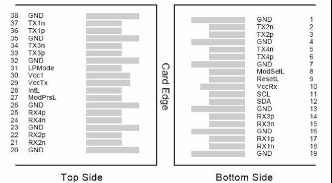
Pin | Symbol | Name/D escription | NOTE |
1 | GND | Transmitter Ground(CommonwithReceiverGround) | 1 |
2 | Tx2n | Transmitter Inverted DataInput |
|
3 | Tx2p | Transmitter Non-Inverted Dat aoutput |
|
4 | GND | Transmitter Ground(CommonwithReceiverGround) | 1 |
5 | Tx4n | Transmitter Inverted DataInput |
|
6 | Tx4p | TransmitterNon-Inverted Datao utput |
|
7 | GND | Transmitter Ground (Common with Receiver Ground) | 1 |
8 | Mod SelL | Module Select |
|
9 | Re setL | Module Reset |
|
10 | Vcc Rx | 3.3V Power Supply Receiver | 2 |
11 | SCL | 2-Wire serial Interface Clock |
|
12 | SDA | 2-Wire serial Interface Data |
|
13 | GND | Transmitter Ground (CommonwithReceiverGround) |
|
14 | Rx3p | Receiver Non-Inverted Data Output |
|
15 | Rx3n | Receiver Inverted Data Output |
|
16 | GND | Transmitter Ground (Common with Receiver Ground) | 1 |
17 | Rx1p | Receiver Non-Inverted Data Output |
|
18 | Rx1n | Receiver Inverted Data Output |
|
19 | GND | Transmitter Ground (Common with Receiver Ground) | 1 |
20 | GND | Transmitter Ground (Common with ReceiverGround) | 1 |
21 | Rx2n | Receiver Inverted Data Output |
|
22 | Rx2p | Receiver Non-Inverted Data Output |
|
23 | GND | Transmitter Ground (Common with Receiver Ground) | 1 |
24 | Rx4n | ReceiverInverted Data Output | 1 |
25 | Rx4p | Receiver Non-Inverted Data Output |
|
26 | GND | Transmitter Ground (Common with Receiver Ground) | 1 |
27 | ModPrsl | Module Present |
|
28 | IntL | Interrupt |
|
29 | VccTx | 3.3V power supply transmitter | 2 |
30 | Vcc1 | 3.3V power supply | 2 |
31 | LPMode | Low Power Mode |
|
32 | GND | Transmitter Ground (Common with Receiver Ground) | 1 |
33 | Tx3p | Transmitter Non-Inverted Data Input |
|
34 | Tx3n | Transmitter Inverted Data Output |
|
35 | GND | Transmitter Ground (Common with Receiver Ground) | 1 |
36 | Tx1p | Transmitter Non-Inverted Data Input |
|
37 | Tx1n | Transmitter Inverted Data Output |
|
38 | GND | Transmitter Ground (Common with Receiver Ground) | 1 |
Notes:
1. GND is the symbol for signal and supply (power) common for QSFP+ modules. All are common within the QSFP+ module and all module voltages are referenced to this potential unless otherwise noted. Connect these directly to the host board signal common ground plane.
2. VccRx, Vcc1 and VccTx are the receiving and transmission power suppliers and shall be applied concurrently. Recommended host board power supply filtering is shown below. Vcc Rx, Vcc1 and Vcc Tx may be internally connected within the QSFP+ transceiver module in any combination. The connector pins are each rated for a maximum current of 500mA.
Digital Diagnostic Functions
SOPTO SPT-QSFP-LR4 supports the 2-wire serial communication protocol as defined in the QSFP+ MSA, which allows real-time access to the following operating parameters:
Transceiver temperature
Laser bias current
Transmitted optical power
Received optical power
Transceiver supply voltage
It also provides a sophisticated system of alarm and warning flags, which may be used to alert end-users when particular operating parameters are outside of a factory-set normal range. The operating and diagnostics information is monitored and reported by a Digital Diagnostics. Transceiver Controller (DDTC) inside the transceiver, which is accessed through the 2-wire serial interface. When the serial protocol is activated, the serial clock signal (SCL pin) is generated by the host.
The positive edge clocks data into the QSFP+ transceiver into those segments of its memory map that are not write-protected. The negative edge clocks data from the QSFP+ transceiver. The serial data signal (SDA pin) is bi-directional for serial data transfer. The host uses SDA in conjunction with SCL to mark the start and end of serial protocol activation. The memories are organized as a series of 8-bit data words that can be addressed individually or sequentially. The 2-wire serial interface provides sequential or random access to the 8 bit parameters, addressed from 000h to the maximum address of the memory.
This clause defines the Memory Map for QSFP transceiver used for serial ID, digital monitoring and certain control functions. The interface is mandatory for all QSFP devices. The memory map has been changed in order to accommodate 4 optical channels and limit the required memory space. The structure of the memory is shown in Figure 2 -QSFP+ Memory Map. The memory space is arranged into a lower, single page, address space of 128 bytes and multiple upper address space pages.
This structure permits timely access to addresses in the lower page, e.g. Interrupt Flags and Monitors. Less time critical entries, e.g. serial ID information and threshold settings are available with the Page Select function. The structure also provides address expansion by adding additional upper pages as needed. For example, in Figure 29 upper pages 01 and 02 are optional. Upper page 01 allows implementation of Application Select Table, and upper page 02 provides user read/write space.
The lower page and upper pages 00 and 03 are always implemented. The interface address used is A0xh and is mainly used for time critical data like interrupt handling in order to enable a “one-time-read” for all data related to an interrupt situation. After an Interrupt, IntL, has been asserted, the host can read out the flag field to determine the effected channel and type of flag.
For more detailed information including memory map definitions, please see the QSFP+ MSA Specification.
Figure2.QSFP Memory Map
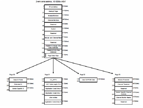
Lower Memory Map
The lower 128 bytes of the 2-wire serial bus address space, see Table 1, is used to access a variety of measurements and diagnostic functions, a set of control functions, and a means to select which of the various upper memory map pages are accessed on subsequent reads. This portion of the address space is always directly addressable and thus is chosen for monitoring and control functions that may need to be repeatedly accessed. The definition of identifier field is the same as page 00h Byte 128.
Table 1— Lower Memory Map
ByteAddress | Description | Type |
0 | Identifier(1Byte) | Read-Only |
1-2 | Status(2Bytes) | Read-Only |
3-21 | Interrupt Flags(19Bytes) | Read-Only |
22-33 | Module Monitors(12Bytes) | Read-Only |
34-81 | Channel Monitors(48Bytes) | Read-Only |
82-85 | Reserved(4Bytes) | Read-Only |
86-97 | Control(12Bytes) | Read/Write |
98-99 | Reserved(2Bytes) | Read/Write |
100-106 | Moduleand Channel Masks(7Bytes) | Read/Write |
107-118 | Reserved(12Bytes) | Read/Write |
119-122 | Password Change Entry Area(optional)(4Bytes) | Read/Write |
123-126 | Password Entry Area(optional)(4Bytes) | Read/Write |
127 | Page Select Byte | Read/Write |
Status Indicator Bits
The Status Indicators are defined in Table 2.
Byte | Bit | Name | Description |
1 | All | Reserved |
|
2 | 7 | Reserved |
|
| 6 | Reserved |
|
| 5 | Reserved |
|
| 4 | Reserved |
|
| 3 | Reserved |
|
| 2 | Reserved |
|
| 1 | IntL | Digital state of the IntL interrupt output pin. |
| 0 | Data_Not_Ready | Indicates transceiver has not yet achieved power up and monitor data is not ready. Bitre mains high until data is ready to be readat which time the device sets the bit low. |
Interrupt Flags
A portion of the memory maps (Bytes 3 through 21), form a flag field. Within this field, the status of LOS and Tx Fault as well as alarms and warnings for the various monitored items is reported. For normal operation and default state, the bits in this field have the value of 0b. For the defined conditions of LOS, Tx Fault, module and channel alarms and warnings, the appropriate bit or bits are set, value = 1b. Once asserted, the bits remained set (latched) until cleared by a read operation that includes the affected bit or reset by the ResetL pin. The Channel Status Interrupt Flags are defined in Table 3.
Byte | Bit | Name | Description |
3 | 7 | L-Tx4 LOS | Latched TX LOS indicator, channel 4 (Not support) |
| 6 | L-Tx3 LOS | Latched TX LOS indicator, channel 3 (Not support) |
| 5 | L-Tx2 LOS | Latched TX LOS indicator, channel2 (Not support) |
| 4 | L-Tx1 LOS | Latched TX LOS indicator, channel1 (Not support) |
| 3 | L-Rx4 LOS | Latched RX LOS indicator, channel4 |
| 2 | L-Rx3 LOS | Latched RX LOS indicator, channel3 |
| 1 | L-Rx2 LOS | Latched RX LOS indicator, channel2 |
| 0 | L-Rx1 LOS | Latched RX LOS indicator, channel1 |
4 | 7-4 | Reserved |
|
| 3 | L-Tx4 Fault | Latched TX fault indicator, channel 4 |
| 2 | L-Tx3 Fault | Latched TX fault indicator, channel 3 |
| 1 | L-Tx2 Fault | Latched TX fault indicator, channel 2 |
| 0 | L-Tx1 Fault | Latched TX fault indicator, channel 1 |
5 | All | Reserved |
|
The Module Monitor Interrupt Flags are defined in Table4.
Byte | Bit | Name | Description |
6 | 7 | L-Temp High Alarm | Latched high temperature alarm |
| 6 | L-Temp Low Alarm | Latched low temperature alarm |
| 5 | L-Temp High Warning | Latched high temperature warning |
| 4 | L-Temp Low Warning | Latched low temperature warning |
| 3-0 | Reserved |
|
7 | 7 | L-Vcc High Alarm | Latched high supply voltage alarm |
| 6 | L-Vcc Low Alarm | Latched low supply voltage alarm |
| 5 | L-Vcc High Warning | Latched high supply voltage warning |
| 4 | L-Vcc Low Warning | Latched low supply voltage warning |
| 3-0 | Reserved |
|
8 | All | Reserved |
|
The Channel Monitor Interrupt Flags are defined in Table 5
Byte | Bit | Name | Description |
9 | 7 | L-Rx1 Power High Alarm | Latched high RX power alarm, channel1 |
| 6 | L-Rx1 Power Low Alarm | Latched low RX power alarm, channel1 |
| 5 | L-Rx1 Power High Warning | Latched high RX power warning, channel1 |
| 4 | L-Rx1 Power Low Warning | Latched low RX power warning, channel1 |
| 3 | L-Rx2 Power High Alarm | Latched high RX power alarm, channel2 |
| 2 | L-Rx2 Power Low Alarm | Latched low RX power alarm, channel2 |
| 1 | L-Rx2 Power High Warning |