
- Sopto Home
-

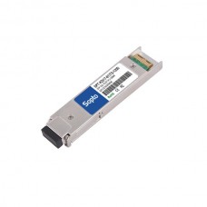
- SPT-XD(17-61)TG-120D 120km DWDM XFP Optical Transceiver
- Fiber Optic Transceiver Module
- High Speed Cable
- Fiber Optical Cable
- Fiber Optical Patch Cords
- Splitter CWDM DWDM
- PON Solution
- FTTH Box ODF Closure
- PCI-E Network Card
- Network Cables
- Fiber Optical Adapter
- Fiber Optical Attenuator
- Fiber Media Converter
- PDH Multiplexers
- Protocol Converter
- Digital Video Multiplexer
- Fiber Optical Tools
- Compatible
SPT-XD(17-61)TG-120D 120km DWDM XFP Optical Transceiver

SPT-XD(17-61)TG-120D
120km DWDM XFP Optical Transceiver
Features
- Wavelength selectable to C-band ITU-T grid wavelengths
- Suitable for use in 100GHz channel spacing DWDM systems
- XFP MSA Rev 4.5 Compliant
- Data rate from 9.95Gbps to 11.3Gbps
- Cooled EML and APD receiver
- link length up to 120km
- Low Power Dissipation 3.5W Maximum
- XFI and line side loopback Mode Supported
- -5ºC to 70ºC Operating Case Temperature
- Diagnostic Performance Monitoring of module temperature,
- Supply Voltages, laser bias current, transmit optical power, and receive optical power
- RoHS6 compliant (lead free)
Applications
- SONET OC-192&SDH STM 64
- Ethernet (10GBASE and 10GBASE with FEC)
- DWDM Networks
Description
120km XFP Transceiver exhibits excellent wavelength stability, supporting operation at 100GHz channel, cost effective module. It is designed for 10G SDH/SONET and 10G Ethernet applications.
The transmitter section incorporates a coded EML laser, and the receiver section consists of an APD photodiode integrated with a TIA, Integrated low power dual CDR with Electronic Dispersion Compensation (EDC). This module can be used to compensate channel impairments caused by either single mode fiber up to 120 km .All modules satisfy class I laser safety requirements. XFP transceiver provides an enhanced monitoring interface, which allows real-time access to device operating parameters such as transceiver temperature, laser bias current, transmitted optical power, and received optical power and transceiver supply voltage.
Module Block Diagram
.jpg)
Absolute Maximum Ratings
|
Parameter |
Symbol |
Min |
Max |
Unit |
|
Supply Voltage1 |
Vcc3 |
-0.5 |
4.0 |
V |
|
Supply Voltage2 |
Vcc5 |
-0.5 |
6.0 |
V |
|
Supply Voltage3 |
Vcc2 |
-0.5 |
2 |
V |
|
Storage Temperature |
Tst |
-40 |
85 |
ºC |
|
Case Operating Temperature |
Top |
-5 |
70 |
ºC |
Operating Conditions
|
Parameter |
Symbol |
Min |
Typical |
Max |
Unit |
|
Supply Voltage1 |
Vcc3 |
3.13 |
3.3 |
3.47 |
V |
|
Supply Current1 |
Icc3 |
- |
- |
750 |
mA |
|
Supply Voltage2 |
Vcc5 |
4.75 |
5 |
5.25 |
V |
|
Supply Current2 |
Icc5 |
- |
- |
500 |
mA |
|
Supply Voltage3 |
Vcc2 |
1.71 |
1.8 |
1.89 |
V |
|
Supply Current3 |
Icc2 |
- |
- |
750 |
mA |
|
Operating Case Temperature |
Tca |
-5 |
- |
70 |
ºC |
|
Module Power Dissipation |
Pm |
- |
- |
3.5 |
W |
Transmitter Specifications –Optical
|
Parameter |
Symbol |
Min |
Typical |
Max |
Unit |
|
Center Wavelength-Start of Life[1] |
λc |
λc-25 |
λc |
λc+25 |
pm |
|
Center Wavelength-End of Life[1] |
λc |
λc-100 |
λc |
λc+100 |
pm |
|
Optical Transmit Power |
Po |
-2 |
- |
+3 |
dBm |
|
Optical Transmit Power (disabled) |
PTX_DIS |
- |
- |
-30 |
dBm |
|
Extinction Ratio |
ER |
9 |
- |
- |
dB |
|
Jitter Generation(P-P) |
JGP-P |
- |
- |
0.1 |
UI |
|
Jitter Generation(RMS) |
JGRMS |
- |
- |
0.01 |
UI |
|
Spectral Width(-20dB) |
Δλ20 |
- |
- |
0.3 |
nm |
|
Side Mode Suppression Ratio |
SMSR |
30 |
- |
- |
dB |
|
Dispersion penalty(800ps/nm)[2] |
DP |
- |
- |
2 |
dB |
|
Relative Intensity Noise |
RIN |
- |
- |
-130 |
dB/Hz |
|
Eye Mask |
Compliant with ITU-TG.691 STM-64 eye mask |
||||
Notes:
1. Wavelength stability is achieved within 60 seconds (max) of power up.
2. BER=10 -12; PRBS 2 31-1@9.95Gbps.
Transmitter Specifications – Electrical
|
Parameter |
Symbol |
Min |
Typical |
Max |
Unit |
|
Input differential impedance |
Rim |
- |
100 |
- |
Ω |
|
Differential data Input |
VtxDIFF |
120 |
- |
850 |
mV |
|
Transmit Disable Voltage |
VD |
2.0 |
- |
Vcc3+0.3 |
V |
|
Transmit Enable Voltage |
Ven |
0 |
- |
+0.8 |
V |
|
Transmit Disable Assert Time |
Vn |
- |
- |
10 |
us |
Receiver Specifications – Optical
|
Parameter |
Symbol |
Min |
Typical |
Max |
Unit |
|
|
Maximum Input Power |
RX-overload |
-7 |
- |
- |
dBm |
|
|
Input Operating Wavelength |
λ |
1528 |
- |
1565 |
nm |
|
|
Reflectance |
Rrx |
- |
- |
-27 |
dB |
|
|
Loss of Signal Asserted |
LOS_A |
-34 |
- |
- |
dBm |
|
|
LOS De-Asserted |
LOS_D |
- |
- |
-24 |
dBm |
|
|
LOS Hysteresis |
LOS_H |
0.5 |
- |
- |
dB |
|
|
Receiver Sensitivity |
||||||
|
Data rate (Gb/s) |
BER |
Dispersion (ps/nm) |
Sensitivity back-to-back at OSNR>30dB (dBm) |
Power Penalty at OSNR>30dB (dB) |
||
|
9.95~10.7 |
1e-12 |
-500 to 2400 |
-24 |
2 |
||
|
11.1~11.3 |
1e-12 |
-500 to 2400 |
-23 |
2 |
||
|
OSNR Performance |
||||||
|
Data rate (Gb/s) |
BER |
Dispersion (ps/nm) |
Min OSNR Back-to-back at Power: -7 to -18 dBm(dB) |
Max OSNR Penalty at Power: -7 to -18dBm (dB) |
||
|
9.95~10.7 |
1e-12 |
-500 to 1450 |
24 |
4 |
||
|
11.1~11.3 |
1e-4 |
-500 to 1300 |
16 |
4 |
||
Receiver Specifications – Electrical
|
Parameter |
Symbol |
Min |
Typical |
Max |
Unit |
|
Output differential impedance |
Rom |
- |
100 |
-- |
Ω |
|
Differential Output Swing |
Vout P-P |
350 |
- |
850 |
mV |
|
Rise/Fall Time[1] |
Tr/Tf |
24 |
- |
- |
ps |
|
Loss of Signal–Asserted |
VOH |
2 |
- |
Vcc3+0.3- |
V |
|
Loss of Signal–Negated |
VOL |
GND |
- |
GND+0.5 |
V |
Notes:
1. 20%-80%;
Reference Clock
|
Parameter |
Symbol |
Min |
Typical |
Max |
Unit |
|
Clock Differential Input Impedance |
CI |
80 |
100 |
120 |
Ω |
|
Differential Input Amplitude (p-p) |
DCA |
640- |
- |
1600 |
mV |
|
Reference Clock Duty Cycle |
RCY |
40 |
- |
60 |
% |
|
Reference Clock Rise/Fall Time[1] |
Tr/Tf |
200 |
- |
1250 |
ps |
|
Reference Clock Frequency |
fu |
- |
Baud/64 |
- |
MHz |
Mechanical Specifications
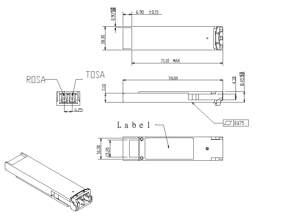
XFP Mechanical Components
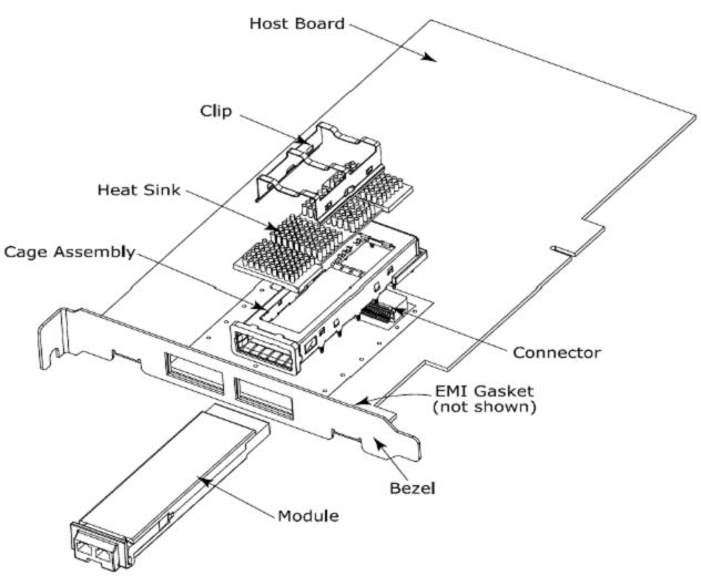
The mechanical components defined:
1. The module, clip and connector dimensions are constant for all applications. While the bezel, cage assembly, EMI gasket and heat sink can be designed and/or adjusted for the individual application.
2. The relatively small form factor of the XFP module combined with an adaptable heat sink option allows host system design optimization of module location, heat sink shape/dimension/fins design, and airflow control. The module can be inserted and removed from the cage with the heat sink and clip attached.
Ordering Information
|
Part Number |
Product Description |
|
SPT-XD(17-61)TG-120D |
XX=ITU Grid 17~61, 10Gbps, DWDM XFP 120km,-5ºC~+70ºC Reference Clock on the Host board |
E-mail:sales@sopto.com