
- Sopto Home
-

- CWDM XFP Optical Transceiver SPT-XC(47-61)TG-80D
- Fiber Optic Transceiver Module
- High Speed Cable
- Fiber Optical Cable
- Fiber Optical Patch Cords
- Splitter CWDM DWDM
- PON Solution
- FTTH Box ODF Closure
- PCI-E Network Card
- Network Cables
- Fiber Optical Adapter
- Fiber Optical Attenuator
- Fiber Media Converter
- PDH Multiplexers
- Protocol Converter
- Digital Video Multiplexer
- Fiber Optical Tools
- Compatible
CWDM XFP Optical Transceiver SPT-XC(47-61)TG-80D

Features
- Wavelength selectable to ITU-T standards covering
- CWDM grid wavelengths
- XFP MSA Compliant
- data rate from 9.95 Gbps to 11.3Gbps
- No Reference Clock required
- Cold EML transmitter and APD receiver
- 1470nm~1570nm link length up to 80km (1600ps/nm)
- 1590nm~1610nm link length up to 70km (1400ps/nm)
- Low Power Dissipation 3.5W Maximum
- -5ºC to 70ºC Operating Case Temperature
- Diagnostic Performance Monitoring of module temperature, supply
- Voltages, laser bias current, transmit optical power, receive optical power
- RoHS compliant and lead free
Applications
- SONET OC-192&SDH STM 64
- 10G Ethernet
- 80 km 10G Fiber Channel
- CWDM Networks
SOPTO CWDM XFP Transceiver exhibits excellent wavelength stability, cost effective module. It is designed for 10G CWDM SDH, 10GBASE-ZR/EW and 10G Fiber- Channel applications. The transceiver consists of two sections: The transmitter section incorporates a colded EML laser. And the receiver section consists of a APD photodiode integrated with a TIA. All modules satisfy class I laser safety requirements. SOPTO CWDM XFP transceiver provides an enhanced monitoring interface, which allows real-time access to device operating parameters such as transceiver temperature, laser bias current, transmitted optical power, received optical power and transceiver supply voltage.
Absolute Maximum Ratings
|
Parameter |
Symbol |
Min |
Max |
Unit |
|
Supply Voltage 1 |
Vcc3 |
-0.5 |
4.0 |
V |
|
Supply Voltage 2 |
Vcc5 |
-0.5 |
6.0 |
V |
|
Supply Voltage 3 |
Vcc2 |
|
2 |
V |
|
Storage Temperature |
Tst |
-40 |
85 |
ºC |
|
Case Operating Temperature |
Top |
-5 |
70 |
ºC |
|
Optical Input Received Power |
APD-IN |
- |
-8 |
dBm |
Operating Conditions
|
Parameter |
Symbol |
Min |
Typical |
Max |
Unit |
|
Supply Voltage 1 |
Vcc3 |
3.13 |
3.3 |
3.47 |
V |
|
Supply current 1 |
Icc3 |
|
|
750 |
mA |
|
Supply Voltage 2 |
Vcc5 |
4.75 |
5 |
5.25 |
V |
|
Supply current 2 |
Icc5 |
|
|
500 |
mA |
|
Supply Voltage 3 |
Vcc2 |
1.71 |
1.8 |
1.89 |
V |
|
Supply current 3 |
Icc2 |
|
|
750 |
mA |
|
Operating Case temperature |
Tca |
-5 |
- |
70 |
ºC |
|
Module Power Dissipation |
Pm |
- |
|
3.5 |
W |
Transmitter Specifications – Optical
|
Parameter |
Symbol |
Min |
Typical |
Max |
Unit |
|
Data Rate Multirate |
Mra |
9.95 |
- |
11.1 |
Gbps |
|
Center Wavelength |
ëc |
1464.5 |
ëc |
1617.5 |
nm |
|
Center wavelength stability |
ÄëD |
−6.5 |
|
6.5 |
nm |
|
Optical Transmit Power |
Po |
0 |
- |
+4 |
dBm |
|
Optical Transmit Power (disabled) |
PTX_DISABLE |
- |
- |
-30 |
dBm |
|
Extinction Ratio |
ER |
9 |
|
- |
dB |
|
Channel Spacing |
∆f |
- |
20 |
- |
nm |
|
Jitter Generation |
TJP-P |
- |
- |
0.1 |
UI |
|
Spectral Width (-20dB) |
Dl20 |
- |
0.1 |
0.3 |
nm |
|
Side Mode Suppression Ratio |
SMSR |
30 |
- |
- |
dB |
|
Dispersion penalty(800ps/nm) |
DP |
|
|
2 |
dB |
|
Eye Mask |
Compliant with ITU-T G.691 STM-64 eye mask |
||||
△Laser- Start of Life
▲Laser End of life
Transmitter Specifications – Electrical
|
Parameter |
Symbol |
Min |
Typical |
Max |
Unit |
|
Input differential impedance |
Rim |
- |
100 |
- |
Ω |
|
Differential data Input |
VtxDIFF |
120 |
- |
850 |
mV |
|
Transmit Disable Voltage |
VD |
2.0 |
- |
Vcc3+0.3 |
V |
|
Transmit Enable Voltage |
Ven |
0 |
- |
+0.8 |
V |
|
Transmit Disable Assert Time |
Vn |
- |
- |
10 |
us |
Receiver Specifications – Optical
|
Parameter |
Symbol |
Min |
Typical |
Max |
Unit |
|
Data Rate Multirate |
Mra |
9.95 |
- |
11.1 |
Gbps |
|
Receiver Sensitivity 9.95Gb/s |
Rsens9 |
- |
- |
-24 |
dBm |
|
Receiver Sensitivity 10.7Gb/s |
Rsens10 |
- |
- |
-23 |
dBm |
|
Maximum Input Power |
RX-overload |
- |
- |
-7 |
dBm |
|
Input Operating Wavelength |
λ |
1260 |
- |
1620 |
nm |
|
Reflectance |
Rrx |
- |
- |
-27 |
dB |
|
Loss of Signal Asserted |
|
-34 |
- |
- |
dBm |
|
LOS De-Asserted |
|
- |
- |
-24 |
dBm |
|
LOS Hysteresis |
|
0.5 |
- |
- |
dB |
Receiver Specifications – Electrical
|
Parameter |
Symbol |
Min |
Typical |
Max |
Unit |
|
Differential Output Swing |
Vout P-P |
350 |
- |
850 |
mV |
|
Rise/Fall Time |
Tr / Tf |
24 |
- |
- |
ps |
|
Loss of Signal –Asserted |
VOH |
2 |
- |
Vcc3+0.3- |
V |
|
Loss of Signal –Negated |
VOL |
0 |
- |
+0.4 |
V |
Low Speed Electrical Signal Timings
|
Parameter |
Symbol |
Min |
Typical |
Max |
Unit |
|
TX Disable, Power_Down/RST |
VIH |
2.0 |
|
Vcc3+0.3 |
V |
|
VIL |
-0.3 |
|
0.8 |
V |
|
|
Interrupt, Mod_NR, Rx_Los |
VOH |
Vdd3-0.5 |
|
Vdd3+0.3 |
V |
|
VOL |
0 |
|
0.4 |
V |
|
|
SCL,SDA(IN) |
VIH |
Vdd3*0.7 |
|
Vdd3+0.5 |
V |
|
VIL |
-0.3 |
|
Vdd3*0.3 |
V |
|
|
SCL,SDA(OUT) |
VOH |
Vdd3-0.5 |
|
Vdd3+0.3 |
V |
|
VOL |
0 |
|
0.4 |
V |
|
|
I2C clock rate |
t_reset |
|
- |
400 |
KHz |
|
Leakage current |
IL |
- |
- |
100 |
uA |
Pin Descriptions
|
Pin |
Logic |
Symbol |
Name/Description |
Ref. |
|
1 |
|
GND |
Module Ground |
1 |
|
2 |
|
VEE5 |
Optional –5.2 Power Supply – Not required |
|
|
3 |
LVTTL-I |
Mod-Desel |
Module De-select; When held low allows the module to , respond to 2-wire serial interface commands |
|
|
4 |
LVTTL-O |
Interrupt |
Interrupt (bar); Indicates presence of an important condition which can be read over the serial 2-wire interface |
2 |
|
5 |
LVTTL-I |
TX_DIS |
Transmitter Disable; Transmitter laser source turned off |
|
|
6 |
|
VCC5 |
+5 Power Supply |
|
|
7 |
|
GND |
Module Ground |
1 |
|
8 |
|
VCC3 |
+3.3V Power Supply |
|
|
9 |
|
VCC3 |
+3.3V Power Supply |
|
|
10 |
LVTTL-I |
SCL |
Serial 2-wire interface clock |
2 |
|
11 |
LVTTL- I/O |
SDA |
Serial 2-wire interface data line |
2 |
|
12 |
LVTTL-O |
Mod_Abs |
Module Absent; Indicates module is not present. Grounded in the module. |
2 |
|
13 |
LVTTL-O |
Mod_NR |
Module Not Ready; |
2 |
|
14 |
LVTTL-O |
RX_LOS |
Receiver Loss of Signal indicator |
2 |
|
15 |
|
GND |
Module Ground |
1 |
|
16 |
|
GND |
Module Ground |
1 |
|
17 |
CML-O |
RD- |
Receiver inverted data output |
|
|
18 |
CML-O |
RD+ |
Receiver non-inverted data output |
|
|
19 |
|
GND |
Module Ground |
1 |
|
20 |
|
VCC2 |
+1.8V Power Supply |
|
|
21 |
LVTTL-I |
P_Down/R ST |
Power Down; When high, places the module in the low power stand-by mode and on the falling edge of P_Down initiates a module reset |
|
|
Reset; The falling edge initiates a complete reset of the module including the 2-wire serial interface, equivalent to a power cycle. |
|
|||
|
22 |
|
VCC2 |
+1.8V Power Supply |
|
|
23 |
|
GND |
Module Ground |
1 |
|
24 |
PECL-I |
RefCLK+ |
Reference Clock non-inverted input, AC coupled on the host board – Not required |
3 |
|
25 |
PECL-I |
RefCLK- |
Reference Clock inverted input, AC coupled on the host board – Not required |
3 |
|
26 |
|
GND |
Module Ground |
1 |
|
27 |
|
GND |
Module Ground |
1 |
|
28 |
CML-I |
TD- |
Transmitter inverted data input |
|
|
29 |
CML-I |
TD+ |
Transmitter non-inverted data input |
|
|
30 |
|
GND |
Module Ground |
1 |
Notes:
1. Module circuit ground is isolated from module chassis ground within the module.
2. Open collector; should be pulled up with 4.7k – 10k ohms on host board to a voltage between 3.15Vand 3.6V.
3. A Reference Clock input is not required.
.png)
Figure1.Electrical Pin-out Details
Digital Diagnostic Functions
SPT-XC(XX-XX)TG-80D Small Form Factor 10Gb/s (XFP) transceivers are compliant with the current XFP Multi-Source Agreement (MSA) Specification Rev 4.5.
As defined by the XFP MSA, SOPTO XFP transceivers provide digital diagnostic functions via a 2-wire serial interface, which allows real-time access to the following operating parameters:
- Transceiver temperature
- Laser bias current
- Transmitted optical power
- Received optical power
- Transceiver supply voltage
It also provides a sophisticated system of alarm and warning flags, which may be used to alert end-users when particular operating parameters are outside of a factory-set normal range.
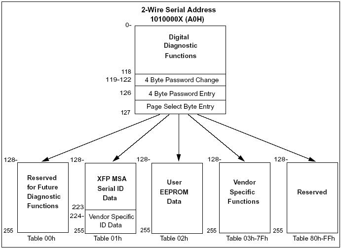
Figure1.2-wire Serial Digital Diagnostic Memory Map
The operating and diagnostics information is monitored and reported by a Digital Diagnostics Transceiver Controller inside the transceiver, which is accessed through the 2-wire serial interface. When the serial protocol is activated, the serial clock signal (SCL pin) is generated by the host. The positive edge clocks data into the XFP transceiver into those segments of its memory map that are not write-protected. The negative edge clocks data from the XFP transceiver. The serial data signal (SDA pin) is bi-directional for serial data transfer. The host uses SDA in conjunction with SCL to mark the start and end of serial protocol activation. The memories are organized as a series of 8-bit data words that can be addressed individually or sequentially. The 2-wire serial interface provides sequential or random access to the 8 bit parameters, addressed from 000h to the maximum address of the memory.
EEPROM Serial ID Memory Contents (Table 01h):
|
Data Address |
Field Size (Bytes) |
Name of Field |
Description and Contents |
|
Base ID Fields |
|||
|
128 |
1 |
Identifier |
Type of Serial transceiver (06h=XFP) |
|
129 |
1 |
Ext. Identifier |
TX Ref Clock Input not Required (90h) |
|
130 |
1 |
Connector |
Code of optical connector type (07h=LC) |
|
131-138 |
8 |
Transceiver |
10GBASE-ZR |
|
139 |
1 |
Encoding |
NRZ(10h) |
|
140 |
1 |
BR-MIN |
9.953Gbps(63h) |
|
141 |
1 |
BR-MAX |
11.3Gbps(71h) |
|
142 |
1 |
Length(SMF)-km |
70KM(46h) or 80KM(50h) |
|
143 |
1 |
Length(E-50um) |
(00h) |
|
144 |
1 |
Length(50um) |
(00h) |
|
145 |
1 |
Length(62.5um) |
(00h) |
|
146 |
1 |
Length(Copper) |
(00h) |
|
147 |
1 |
Device Tech |
Cooled1550nm EML, APD Detector |
|
148-163 |
16 |
Vendor Name |
XFP vendor name: “SOPTO” (ASCII) |
|
164 |
1 |
CDR Support |
CDR supports 9.953Gbps~11.1Gbps(F8h) |
|
165-167 |
3 |
Vendor OUI |
XFP transceiver vendor OUI ID |
|
168-183 |
16 |
Vendor PN |
Part Number: “SPT-XC(XX-XX)TG-80D” (ASCII) |
|
184-185 |
2 |
Vendor rev |
“32 61” means 2a revision (ASCII) |
|
186-187 |
2 |
Wavelength |
Specified ITU Grid Wavelength |
|
188-189 |
2 |
Wavelength Tolerance |
+/-0.025nm |
|
190 |
1 |
Max Case Temp |
70°C(46h) |
|
191 |
1 |
CC_BASE |
Check sum of bytes 128~190 |
|
192-195 |
4 |
Power Supply |
3.5W(MAX) (AF 96 A7 01) |
|
196-211 |
16 |
Vendor SN |
Serial number (ASCII) |
|
212-219 |
8 |
Date code |
Year(2 bytes), Month(2 bytes), Day (2 bytes) |
|
220 |
1 |
Diagnostic type |
No BER Support, Average Power(08h) |
|
221 |
1 |
Enhanced option |
Optional Soft Tx_Disable and P_Down(60h) |
|
222 |
1 |
Aux Monitoring |
+5.0V and +3.3V Supply Voltage(67h) |
|
223 |
1 |
CC_EXT |
Check sum of bytes 192~222 |
|
Vendor Specific ID fields |
|||
|
224-255 |
32 |
Vendor specific |
Vendor specific |
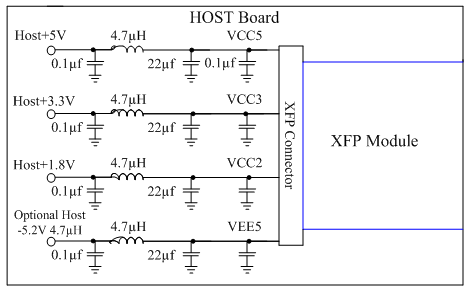
Figure3. Recommended Host Board Power Supply Circuit
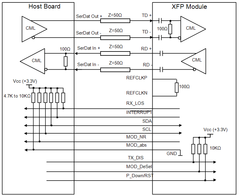
Figure4. Recommended High-speed Interface Circuit
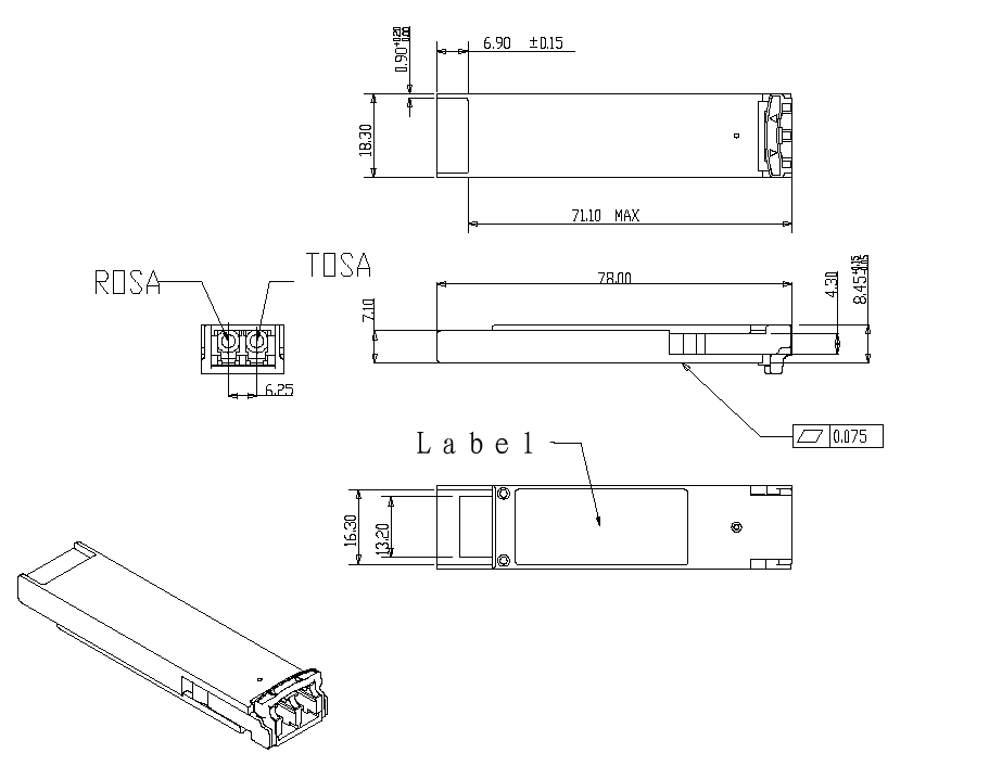
Figure6. Mechanical Specifications
Ordering information
|
Part Number |
Product Description |
|
SPT-XC47TG-80D |
1470nm, 10Gbps, CWDM XFP 80km, -5ºC ~ +70ºC |
|
SPT-XC49TG-80D |
1490nm, 10Gbps, CWDM XFP 80km, -5ºC ~ +70ºC |
|
SPT-XC51TG-80D |
1510nm, 10Gbps, CWDM XFP 80km, -5ºC ~ +70ºC |
|
SPT-XC53TG-80D |
1530nm, 10Gbps, CWDM |