
- Sopto Home
-

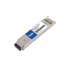
- 10G CWDM XFP,Optical Transceiver,10km SPT-XC(XX)TG-10D
- Fiber Optic Transceiver Module
- High Speed Cable
- Fiber Optical Cable
- Fiber Optical Patch Cords
- Splitter CWDM DWDM
- PON Solution
- FTTH Box ODF Closure
- PCI-E Network Card
- Network Cables
- Fiber Optical Adapter
- Fiber Optical Attenuator
- Fiber Media Converter
- PDH Multiplexers
- Protocol Converter
- Digital Video Multiplexer
- Fiber Optical Tools
- Compatible
10G CWDM XFP,Optical Transceiver,10km SPT-XC(XX)TG-10D

Features
- Supports 9.95Gb/s to 11.1Gb/s bit rates
- Hot-pluggable XFP footprint
- Maximum link length of 10km with SMF
- 4-Wavelengths Uncooled CWDM DFB laser from1270nm to 1330nm, with Step 20nm
- XFP MSA package with duplex LC connector
- No reference clock required
- Compatible with RoHS
- +3.3V power supply
- Power dissipation <2.5W
- Built-in digital diagnostic functions
- Temperature range 0°C to 70°C
Applications
- SDH STM I-64.1 at 9.953Gbps
- 10GBASE-LR/LW 10G Ethernet
- 1200-SM-LL-L 10G Fibre Channel
- 10GE over G.709 at 11.09Gbps
- OC192 over FEC at 10.709Gbps
- Other optical links, up to 11.1Gbps
Description
SPT-XC (XX) TG-10 is compliant with the 10G Small Form-Factor Pluggable (XFP) Multi-Source Agreement (MSA), supporting data-rate of 10.3125Gbps(10GBASE-LR) or 9.953Gbps 10GBASE-LW), and transmission distance up to 10km on SMF. The transceiver module comprises a transmitter with uncooled CWDM DFB laser and a receiver with a PIN photodiode. Transmitter and receiver are separate within a wide temperature range of 0℃ to +70℃and offers optimum heat dissipation and excellent electromagnetic shielding thus enabling high portdensities for 10 GbE systems.
Absolute Maximum Ratings
|
Parameter |
Symbol |
Min |
Max |
Unit |
Ref. |
|
Storage Ambient Temperature Range |
|
-40 |
+85 |
℃ |
|
|
Powered case Temperature Range |
|
0 |
+75 |
℃ |
|
|
Operating Relative Humidity |
RH |
|
80 |
% |
|
|
Supply Voltage Range @ 3.3V |
Vcc3 |
-0.5 |
4.0 |
V |
|
Any stress beyond the maximum ratings can result in permanent damage. The device specifications are guaranteed only
under the recommended operating conditions.
Electrical Characteristics
|
Parameter |
Symbol |
Min |
Typ |
Max |
Unit |
Note |
||
|
Operating Case Temperature Range |
Tc |
0 |
|
+70 |
℃ |
|
||
|
Power Supply Voltage @ 3.3V |
Vcc3 |
3.13 |
3.3 |
3.47 |
V |
|
||
|
Module total power |
P |
|
|
2.5 |
W |
|
||
|
Transmitter |
||||||||
|
Input differential impedance |
Rin |
|
100 |
|
Ω |
1 |
||
|
Differential data input swing |
Vin,pp |
120 |
|
820 |
mV |
|
||
|
Transmit Disable Voltage |
VD |
2.0 |
|
Vcc |
V |
|
||
|
Transmit Enable Voltage |
VEN |
GND |
|
GND+0.8 |
V |
|
||
|
Transmit Disable Assert Time |
|
|
|
10 |
us |
|
||
|
Receiver |
||||||||
|
Differential data output swing |
Vout,pp |
500 |
|
850 |
mV |
|
||
|
Data output rise time |
tr |
|
|
38 |
ps |
2 |
||
|
Data output fall time |
tf |
|
|
38 |
ps |
2 |
||
|
LOS Fault |
VLOS fault |
Vcc - 0.5 |
|
VccHOST |
V |
3 |
||
|
LOS Normal |
VLOS norm |
GND |
|
GND+0.5 |
V |
3 |
||
|
Power Supply Rejection |
PSR |
See Note 3 below |
4 |
|||||
Notes:
1. After internal AC coupling.
2. 20 – 80 %
3. Loss Of Signal is open collector to be pulled up with a 4.7k – 10kohm resistor to 3.15 – 3.6V. Logic 0 indicates normal
operation; logic 1 indicates no signal detected.
4. Per Section 2.7.1. in the XFP MSA Specification.
Optical Characteristics
|
Parameter |
Symbol |
Min |
Typ |
Max |
Unit |
Ref. |
|
Transmitter |
||||||
|
Optical output Power |
P |
-6.5 |
|
+0.5 |
dBm |
|
|
Optical Wavelength |
λ |
1270 |
|
1330 |
nm |
|
|
Optical Extinction Ratio |
ER |
6 |
|
|
dB |
1 |
|
Side Mode Suppression Ratio |
SMSR |
30 |
|
|
dB |
|
|
Average Launch power of OFF transmitter |
POFF |
-30 |
|
|
dBm |
|
|
Tx Jitter |
Txj |
Compliant with each standard requirements |
|
|||
|
Receiver |
||||||
|
Receiver Sensitivity |
RSENS |
|
-16 |
-14.5 |
dBm |
2 |
|
Receiver Sensitivity in OMA |
RSENS |
|
|
-12.5 |
dBm |
2 |
|
Maximum Input Power |
PMAX |
+0.5 |
|
|
dBm |
|
|
Optical Center Wavelength |
λC |
1260 |
|
1600 |
nm |
|
|
LOS De-Assert |
LOSD |
|
|
-15 |
dBm |
|
|
LOS Assert |
LOSA |
-25 |
|
|
dBm |
|
|
LOS Hysteresis |
|
1 |
|
4 |
dB |
|
Notes:
1, PRBS 231-1 test pattern @10.3125Gbps.
2, PRBS 231-1 test pattern @10.3125Gbps, BER≤10-12.
Pin Descriptions
|
Pin |
Logic |
Symbol |
Name/Description |
Ref |
|
1 |
|
GND |
Module Ground |
1 |
|
2 |
|
VEE5 |
Optional –5.2 Power Supply – Not required |
|
|
3 |
LVTTL-I |
Mod-Desel |
Module De-select; When held low allows the module to , respond to 2-wire serial interface commands |
|
|
4 |
LVTTL-O |
Interrupt |
Interrupt (bar); Indicates presence of an important condition which can be read over the serial 2-wire interface |
2 |
|
5 |
LVTTL-I |
TX_DIS |
Transmitter Disable; Transmitter laser source turned off |
|
|
6 |
|
VCC5 |
+5 Power Supply – Not required |
|
|
7 |
|
GND |
Module Ground |
1 |
|
8 |
|
VCC3 |
+3.3V Power Supply |
|
|
9 |
|
VCC3 |
+3.3V Power Supply |
|
|
10 |
LVTTL-I |
SCL |
Serial 2-wire interface clock |
2 |
|
11 |
LVTTL- I/O |
SDA |
Serial 2-wire interface data line |
2 |
|
12 |
LVTTL-O |
Mod_Abs |
Module Absent; Indicates module is not present. Grounded in the module. |
2 |
|
13 |
LVTTL-O |
Mod_NR |
Module Not Ready; |
2 |
|
14 |
LVTTL-O |
RX_LOS |
Receiver Loss of Signal indicator |
2 |
|
15 |
|
GND |
Module Ground |
1 |
|
16 |
|
GND |
Module Ground |
1 |
|
17 |
CML-O |
RD- |
Receiver inverted data output |
|
|
18 |
CML-O |
RD+ |
Receiver non-inverted data output |
|
|
19 |
|
GND |
Module Ground |
1 |
|
20 |
|
VCC2 |
+1.8V Power Supply – Not required |
|
|
21 |
LVTTL-I |
P_Down/R ST |
Power Down; When high, places the module in the low power stand-by mode and on the falling edge of P_Down initiates a module reset |
|
|
Reset; The falling edge initiates a complete reset of the module including the 2-wire serial interface, equivalent to a power cycle. |
|
|||
|
22 |
|
VCC2 |
+1.8V Power Supply – Not required |
|
|
23 |
|
GND |
Module Ground |
1 |
|
24 |
PECL-I |
RefCLK+ |
Reference Clock non-inverted input, AC coupled on the host board – Not required |
3 |
|
25 |
PECL-I |
RefCLK- |
Reference Clock inverted input, AC coupled on the host board – Not required |
3 |
|
26 |
|
GND |
Module Ground |
1 |
|
27 |
|
GND |
Module Ground |
1 |
|
28 |
CML-I |
TD- |
Transmitter inverted data input |
|
|
29 |
CML-I |
TD+ |
Transmitter non-inverted data input |
|
|
30 |
|
GND |
Module Ground |
1 |
Notes:
1. Module circuit ground is isolated from module chassis ground within the module.
2. Open collector; should be pulled up with 4.7k – 10k ohms on host board to a voltage between 3.15Vand 3.6V.
3. A Reference Clock input is not required.
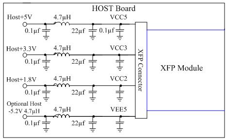
Host board Connector Pinout
.png)
General Specifications
|
Parameter |
Symbol |
Min |
Typ |
Max |
Units |
Ref. |
|
Bit Rate |
BR |
9.95 |
|
11.1 |
Gb/s |
1 |
|
Bit Error Ratio |
BER |
|
|
10-12 |
|
2 |
|
Max. Supported Link Length |
LMAX |
|
10 |
|
km |
1 |
Notes:
1. SONET OC-192 SR-1,SDH STM I-64.1 ,10GBASE-LR/LW, 1200-SM-LL-L
2. Tested with a 231 – 1 PRBS
Management Interface
The transceivers provide serial ID memory contents and diagnostic information about the present operating conditions by the 2-wire serial interface (SCL, SDA).
The Module provides diagnostic information about the present operating conditions. The transceiver generates this diagnostic data by digitization of internal analog signals. Alarm/warning threshold data is written during device manufacture. Received power monitoring, transmitted power monitoring, bias current monitoring, supply voltage monitoring and temperature monitoring all are implemented.
The digital diagnostic memory map specific data field defines as following.
TG-80D-1.jpg)
Recommended Host Board Power Supply Circuit
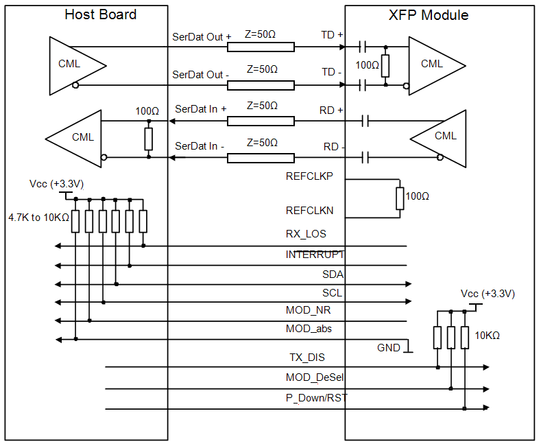
Recommended High-speed Interface Circuit
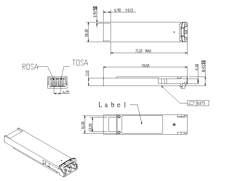
Mechanical Specifications
XFP transceivers are compliant with the dimensions defined by the XFP Multi-Sourcing Agreement (MSA).
Ordering information
|
Part Number |
Product Description |
|
SPT-XC(27-33)TG-10D |
1270nm~1330nm,with step 20nm Uncooled CWDM, 10Gbps, 10km,0ºC ~+70ºC, |
E-mail: sales@sopto.com
Web : http://www.sopto.com