
- Sopto Home
-

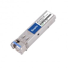
- SPT-P1RV3-LXXD 3Gbps Video SFP Optical Receiver
- Fiber Optic Transceiver Module
- High Speed Cable
- Fiber Optical Cable
- Fiber Optical Patch Cords
- Splitter CWDM DWDM
- PON Solution
- FTTH Box ODF Closure
- PCI-E Network Card
- Network Cables
- Fiber Optical Adapter
- Fiber Optical Attenuator
- Fiber Media Converter
- PDH Multiplexers
- Protocol Converter
- Digital Video Multiplexer
- Fiber Optical Tools
- Compatible
SPT-P1RV3-LXXD 3Gbps Video SFP Optical Receiver
SPT-P1RV3-LXXD
3Gbps Video SFP Optical Receiver, PIN photo detector
Features
HD-SDI SFP Receiver available
SD-SDI SFP Receiver available
3G-SDI SFP Receiver available
SMPTE 297-2006 Compatible.
Metal enclosure for Lower EMI
PIN photo detector
Supports video pathological patterns for SD-SDI, HD-SDI and 3G-SDI
Compliant with SFP MSA and SFF-8472 with duplex LC receptacle
Digital Diagnostic functions available through the I2C interface
Compatible with RoHS
+3.3V single power supply
Operating case temperature: Standard: 0 to +70°C
Applications
SMPTE 297-2006 Compatible Electrical-to-Optical Interfaces.
HDTV/SDTV Service Interfaces.
Description
The video series transceivers are high performance, cost effective modules for duplex video transmission application over single mode fiber.
The receiver is designed to receive data rates from 50Mbps to 2.97Gbps and is specifically designed for robust performance in the presence of SDI pathological patterns for SMPTE 259M, SMPTE 344M, SMPTE 292M and SMPTE 424M serial rates. The module is fully compliant with SMPTE 297M-2006.
The receiver is consists of a PIN photodiode integrated with a trans-impedance preamplifier (TIA) and MCU control unit. All modules satisfy class I laser safety requirements.
The receivers are compatible with SFP Multi-Source Agreement (MSA) and SFF-8472. For further information, please refer to SFP MSA.
Absolute Maximum Ratings
|
Parameter |
Symbol |
Min |
Max |
Unit |
|
Supply Voltage |
Vcc |
-0.5 |
4.5 |
V |
|
Storage Temperature |
Ts |
-40 |
+85 |
°C |
|
Operating Humidity |
- |
5 |
85 |
% |
Recommended Operating Conditions
|
Parameter |
Symbol |
Min |
Typical |
Max |
Unit |
|
|
Operating Case Temperature |
Standard |
Tc |
0 |
|
+70 |
°C |
|
Power Supply Voltage |
Vcc |
3.13 |
3.3 |
3.47 |
V |
|
|
Power Supply Current |
Icc |
|
|
150 |
mA |
|
|
Data Rate |
|
|
3 |
|
Gbps |
|
Optical and Electrical Characteristics
|
Parameter |
Symbol |
Min |
Typical |
Max |
Unit |
Notes |
||
|
Receiver |
||||||||
|
Rise/Fall Time (20%~80%) |
SD-SDI |
tr/tf |
|
|
1500 |
ps |
|
|
|
HD-SDI |
|
|
270 |
1 |
||||
|
3G-SDI |
|
|
135 |
|
||||
|
Total Output jitter |
PRBS and cooler bar |
SD-SDI |
|
|
70 |
200 |
ps |
|
|
HD-SDI |
|
|
50 |
135 |
|
|||
|
3G-SDI |
|
|
70 |
100 |
|
|||
|
pathological |
SD-SDI |
|
|
200 |
300 |
|
||
|
HD-SDI |
|
|
115 |
|
|
|||
|
3G-SDI |
|
|
120 |
|
|
|||
|
Centre Wavelength |
λc |
1260 |
|
1580 |
nm |
|
||
|
Receiver Sensitivity (PRBS) |
SD-SDI |
|
|
|
-22 |
dBm |
|
|
|
HD-SDI |
|
|
|
-22 |
dBm |
|
||
|
3G-SDI |
|
|
|
-22 |
dBm |
|
||
|
Receiver Sensitivity (Pathological) |
SD-SDI |
|
|
|
-20 |
dBm |
|
|
|
HD-SDI |
|
|
|
-22 |
dB |
|
||
|
3G-SDI |
|
|
|
-22 |
mV |
|
||
|
Receiver Overload |
|
0 |
|
|
dBm |
3 |
||
|
LOS De-Assert |
LOSD |
|
|
|
dBm |
|
||
|
LOS Assert |
LOSA |
-29 |
|
|
dBm |
|
||
|
LOS Hysteresis |
|
1 |
|
4 |
dB |
|
||
|
Data Output Swing Differential |
Vout |
650 |
800 |
1000 |
mV |
2 |
||
|
LOS |
High |
|
2.0 |
|
Vcc |
V |
|
|
|
Low |
|
|
|
0.8 |
V |
|
||
Notes:
1. Rise and fall times, 20% to 80%, are measured following a fourth-order Bessel-Thompson filter with a bandwidth of 0.75 x clock frequency corresponding to the serial data rate.
2. PECL input, internally AC-coupled and terminated.
3. Internally AC-coupled
Timing and Electrical
|
Parameter |
Symbol |
Min |
Typical |
Max |
Unit |
|
LOS Assert Time |
t_loss_on |
|
|
100 |
µs |
|
LOS De-assert Time |
t_loss_off |
|
|
100 |
µs |
|
Serial ID Clock Rate |
f_serial_clock |
|
|
280 |
KHz |
|
MOD_DEF(0:2)-High |
VH |
2 |
|
Vcc |
V |
|
MOD_DEF(0:2)-Low |
VL |
|
|
0.8 |
V |
Diagnostics
|
Parameter |
Range |
Unit |
Accuracy |
Calibration |
|
|
Temperature |
0to+70 |
°C |
±3°C |
Internal/External |
|
|
Voltage |
3.0to3.6 |
V |
±3% |
Internal/External |
|
|
RX Power |
-20to-6 |
dBm |
±3dB |
Internal/External |
|
I2C Bus Interface
The I2C bus interface uses the 2-wire serial CMOS E2PROM protocol. The serial interface meets the following specifications:
1. Support a maximum clock rate of 280 KHz.
2. Input/output levels comply with LVCMOS/LVTTL or compatible logics.
Low: 0 – 0.8 V High: 2.0 – 3.3 V Undefined: 0.8 – 2.0 V
Pin Definitions
SFP MSA Type
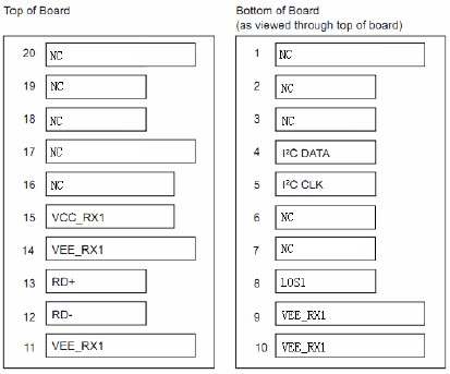
Pin Descriptions (SFP MSA Type)
|
Pin |
Signal Name |
Description |
Plug Seq. |
Notes |
|
1 |
NC |
Not Connected |
|
|
|
2 |
NC |
Not Connected |
|
|
|
3 |
NC |
Not Connected |
|
|
|
4 |
MOD_DEF(2) |
SDA Serial Data Signal |
3 |
Note1 |
|
5 |
MOD_DEF(1) |
SCL Serial Clock Signal |
3 |
Note1 |
|
6 |
NC |
Not Connected |
|
|
|
7 |
NC |
Not Connected |
|
|
|
8 |
LOS |
Loss of Signal |
3 |
Note2 |
|
9 |
VEER |
Receiver Ground |
1 |
|
|
10 |
VEER |
Receiver Ground |
1 |
|
|
11 |
VEER |
Receiver Ground |
1 |
|
|
12 |
RD- |
Inv. Received Data Out |
3 |
Note3 |
|
13 |
RD+ |
Received Data Out |
3 |
Note3 |
|
14 |
VEER |
Receiver Ground |
1 |
|
|
15 |
VCCR |
Receiver Power Supply |
2 |
|
|
16 |
NC |
Not Connected |
|
|
|
17 |
NC |
Not Connected |
|
|
|
18 |
NC |
Not Connected |
|
|
|
19 |
NC |
Not Connected |
|
|
|
20 |
NC |
Not Connected |
|
|
Non Standard Type
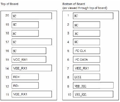
PinDescriptions(NotStandardType)
|
Pin |
Signal Name |
Description |
Plug Seq. |
Notes |
|
1 |
NC |
Not Connected |
|
|
|
2 |
NC |
Not Connected |
|
|
|
3 |
NC |
Not Connected |
|
|
|
4 |
NC |
Not Connected |
|
|
|
5 |
I2CCLK |
SCL Serial Clock Signal |
3 |
Note1 |
|
6 |
I2CDATA |
SDA Serial Data Signal |
3 |
Note1 |
|
7 |
VEE_RX1 |
Receiver1 Ground |
3 |
|
|
8 |
LOS1 |
Loss of Signal |
3 |
Note2 |
|
9 |
VEE_RX1 |
Receiver1 Ground |
1 |
|
|
10 |
VEE_RX1 |
Receiver1 Ground |
1 |
|
|
11 |
VEE_RX1 |
Receiver1 Ground |
1 |
|
|
12 |
RD- |
Inv. Received Data Out |
3 |
Note3 |
|
13 |
RD+ |
Received Data Out |
3 |
Note3 |
|
14 |
VEE_RX1 |
Receiver1 Ground |
1 |
|
|
15 |
VCC_RX1 |
Receiver1 Power Supply |
2 |
|
|
16 |
NC |
Not Connected |
|
|
|
17 |
NC |
Not Connected |
|
|
|
18 |
NC |
Not Connected |
|
|
|
19 |
NC |
Not Connected |
|
|
|
20 |
NC |
Not Connected |
|
|
Notes:
Plug Seq.: Pin engagement sequence during hot plugging.
1) These are the module definition pins. They should be pulled up with a 4.7k~10kΩ resistor on the host board. The pull-up voltage shall be VccR.
I2C CLK is the clock line of two wire serial interface for serial ID
I2C DATA is the data line of two wire serial interface for serial ID
2) LOS is an open collector output, which should be pulled up with a 4.7k~10kΩ resistor. Pull up voltage between 2.0V andVccand0.3V. Logic 1 indicates loss of signal; Logic 0 indicates normal operation. In the low state, the output will be pulled to less than 0.8V.
3) RD-/+: These are the differential receiver outputs. They are internally AC-coupled 100 differential lines which should be terminated with 100Ω (differential) at the user SERDES.
Serial ID Field Memory Map
The module serial Id and calibration information is stored in the E2PROM of the SFP supervising device using the address map.
|
ByteAdder |
BitSize |
Name |
Description |
Value(hex) |
|
0 |
1 |
Identifier |
Type of transceiver |
82 |
|
1 |
1 |
Ext. Identifier |
Extended identifier of type of transceiver |
04 |
|
2 |
1 |
Connector |
Code for connect or type |
07 |
|
3 |
1 |
Standards Compliance |
For SMPTE259M/344M/292M/424M and SMPTE297M |
41 |
|
4-10 |
7 |
Transceiver |
Code for electronic or optical compatibility, Not applicable. |
|
|
11 |
1 |
Encoding |
Code for serial encoding algorithm |
30 |
|
12 |
1 |
BR, Nominal |
Nominal signaling rate, units of 100MBd. |
1E |
|
13 |
1 |
Rate Identifier |
Type of rate select functionality,Not applicable |
|
|
14 |
1 |
Length(SMF,km) |
Link length supported for single mode fiber, units of km |
14 |
|
15 |
1 |
Length(SMF) |
Link length supported for single mode fiber, units of 100m |
00 |
|
16 |
1 |
Length(50um) |
Link length supported for 50um OM2 fiber, units of 10m |
00 |
|
17 |
1 |
Length(62.5um) |
Link length supported for 62.5um OM1 fiber, units of 10m |
00 |
|
18 |
1 |
Length(cable) |
Link length supported for copper or direct attach cable, units of m |
00 |
|
19 |
1 |
Length(OM3) |
Link length supported for 50um OM3 fiber, units of 10m |
00 |
|
20-35 |
16 |
Vendor name |
SFP vendor name (ASCII) |
X |
|
36 |
1 |
Reserved |
Reserved |
00 |
|
37 |
3 |
Vendor OUI |
SFP vendor IEEE company ID |
|
|
38 |
00 |
|||
|
39 |
|
|||
|
40-55 |
16 |
Vendor PN |
Part number providedby SFP vendor(ASCII) |
X |
|
56 |
4 |
Vendor rev |
Revision level for part number provided by vendor (ASCII) |
X |
|
57 |
||||
|
58 |
||||
|
59 |
||||
|
60 |
2 |
Wavelength |
Laser wavelength (Passive / Active Cable Specification Compliance) |
|
|
61 |
|
|||
|
62 |
1 |
Unal located |
|
|
|
63 |
1 |
CC_BASE |
Check code for Base ID Fields |
|
|
64 |
2 |
Options |
Indicates which optional transceiver signal sare implemented |
|
|
65 |
|
|||
|
66 |
1 |
BR,max |
Upper bit rate margin, units of % |
05 |
|
67 |
1 |
BR,min |
Lower bit rate margin, units of % |
5F |
|
68-83 |
16 |
Vendor SN |
Serial number provided by vendor (ASCII) |
X |
|
84 |
|
|
|
|
|
85-91 |
8 |
Date code |
Vendor’s manufacturing date code |
|
|
92 |
1 |
Diagnostic Monitoring Type |
Indicates which type of diagnostic monitoring is implemented (ifany) in the transceiver |
28 |
|
93 |
1 |
Enhanced Options |
Indicates which optional enhanced features are implemented (ifany) in the transceiver |
90 |
|
94 |
1 |
SFF-8472 Compliance |
Indicates which revision of SFF-8472 the transceiver complies with. |
X |
|
95 |
1 |
CC_EXT |
Check code for the Extended ID Fields |
|
|
96-127 |
32 |
Vendor Specific |
Vendor Specific EEPROM |
0 |
Digital Diagnostic Monitoring Interface (2-Wire Address A2H)
|
Byte Addr |
Bit Size |
Name |
Description and Value of the Field |
|
00-01 |
2 |
Temp High Alarm |
MSB at lower address. 100°C |
|
02-03 |
2 |
Temp Low Alarm |
MSB at lower address. -50°C |
|
04-05 |
2 |
Temp High Warning |
MSB at lower address. 95°C |
|
06-07 |
2 |
Temp Low Warning |
MSB at lower address. -45°C |
|
08-09 |
2 |
Voltage High Alarm |
MSB at lower address. 3.7V |
|
10-11 |
2 |
Voltage Low Alarm |
MSB at lower address. 2.9V |
|
12-13 |
2 |
Voltage High Warning |
MSB at lower address. 3.6V |
|
14-15 |
2 |
Voltage Low Warning |
MSB at lower address. 3.0V |
|
16-17 |
2 |
Bias High Alarm |
MSB at lower address. 70mA |
|
18-19 |
2 |
Bias Low Alarm |
MSB at lower address. 8mA |
|
20-21 |
2 |
Bias High Warning |
MSB at lower address. 65mA |
|
22-23 |
2 |
Bias Low Warning |
MSB at lower address. 9mA |
|
24-25 |
2 |
|
|
|
26-27 |
2 |
|
|
|
28-29 |
2 |
|
|
|
30-31 |
2 |
|
|
|
32-33 |
2 |
RX Power High Alarm |
MSB at lower address. 1dBm |
|
34-35 |
2 |
RX Power Low Alarm |
MSB at lower address. -25dBm |
|
36-37 |
2 |
RX Power High Warning |
MSB at lower address. 0dBm |
|
38-39 |
2 |