
- Sopto Home
-

- SPET-X53T1-SX3DA Asymmetric 10G EPON OLT XFP Transceiver
- Fiber Optic Transceiver Module
- High Speed Cable
- Fiber Optical Cable
- Fiber Optical Patch Cords
- Splitter CWDM DWDM
- PON Solution
- FTTH Box ODF Closure
- PCI-E Network Card
- Network Cables
- Fiber Optical Adapter
- Fiber Optical Attenuator
- Fiber Media Converter
- PDH Multiplexers
- Protocol Converter
- Digital Video Multiplexer
- Fiber Optical Tools
- Compatible
SPET-X53T1-SX3DA Asymmetric 10G EPON OLT XFP Transceiver

SPET-X53T1-SX3DA
Asymmetric 10G EPON OLT XFP Transceiver
Features
Single Fiber Transceiver with single mode SC receptacle
1577nm continuous-mode 10.3125G/s transmitter with EML laser
1310nm burst-mode 1.25G/s receiver with APD-TIA
Single 3.3V power supply
LVPECL compatible data input /output
Burst mode received signal strength indication (RSSI) output
Complies with IEEE P802.3™D3.2 10/1GBASE–PRX30
Digital diagnostic interface compliant with SFF-8472 Rev 9.4
Complies with XFP MSA
Complies with RoHS directive
Operating case temperature: Standard: 0 to +70°C
Applications
Asymmetric 10G/1G Ethernet Passive Optical Network OLT
Description
The SPET-X53T1-SX3DA transceiver is the high performance module for single fiber by using 1577nm continuous-mode transmitter and 1310nm burst-mode receiver. It is optical line terminal (OLT) for IEEE P802.3™D3.2 10/1GBASE–PRX30. The optical transceiver is compliant with XFP Multi- Source Agreement (MSA).
The transmitter section uses a 1577nm EML LD with automatic power control (APC) function and temperature compensation circuitry to ensure stable extinction ratio overall operating temperature range. and is ClassⅠlaser compliant IEC825 and CDRH standards.
The receiver has a hermetically packaged APD-TIA (trans-impedance amplifier) pre-amplifier and a limiting amplifier with LVPECL compatible differential outputs. The receiver also supports burst mode RSSI output which is enabled by a trigger. Burst mode RSSI function can satisfy system the demand of monitoring the power from any ONU.
Absolute Maximum Ratings
|
Parameter |
Symbol |
Min. |
Max. |
Units |
Notes |
|
Storage Temperature |
Tst |
-40 |
+85 |
°C |
- |
|
Operating Case Temperature |
Tc |
0 |
70 |
°C |
- |
|
Operating Humidity |
RH |
5 |
90 |
% |
Non-condensing |
|
Input Voltage |
- |
GND |
Vcc |
V |
- |
|
Power Supply Voltage |
Vcc3 |
0 |
3.6 |
V |
- |
|
Power Supply Voltage |
Vcc5 |
0 |
6 |
V |
- |
Recommended Operating Conditions
|
Parameter |
Symbol |
Min |
Typical |
Max |
Unit |
|
|
Operating Case Temperature |
Standard |
Tc |
0 |
|
+70 |
°C |
|
Power Supply Voltage |
Vcc3 |
3.13 |
3.3 |
3.47 |
V |
|
|
Power Supply Voltage |
Vcc5 |
4.75 |
5 |
5.25 |
V |
|
|
Power Supply Current |
Icc3 |
|
|
1000 |
mA |
|
|
Power Supply Current |
Icc5 |
|
|
500 |
mA |
|
Optical and Electrical Characteristics
|
Parameter |
Symbol |
Min |
Typical |
Max |
Unit |
Notes |
|
|
Transmitter |
|||||||
|
Data Rate |
|
|
10.3125 |
|
Gb/S |
|
|
|
Centre Wavelength |
λc |
1575 |
1577 |
1580 |
nm |
|
|
|
Spectral Width |
∆λ |
|
|
1 |
nm |
|
|
|
Side Mode Suppression Ratio |
SMSR |
30 |
|
|
dB |
|
|
|
Average Output Power (BOL) |
Pout |
2 |
|
5 |
dBm |
1 |
|
|
Extinction Ratio |
ER |
6 |
|
|
dB |
|
|
|
Average Launch Power-OFF Transmitter |
Poff |
|
|
-39 |
dBm |
|
|
|
Optical Eye Diagram |
Compliant with IEEEP802.3™D3.2 Figure75–8 |
||||||
|
Optical Rise/ Fall Time (20%~80%) |
tr/tf |
|
|
26 |
ps |
|
|
|
Data Input Swing Differential |
VIN |
200 |
|
1000 |
mV |
2 |
|
|
Input Differential Impedance |
ZIN |
90 |
100 |
110 |
Ω |
|
|
|
TX Disable |
Disable |
|
2.0 |
|
Vcc |
V |
|
|
Enable |
|
0 |
|
0.8 |
V |
|
|
|
Receiver |
|||||||
|
Data Rate |
|
|
1.25 |
|
Gb/S |
|
|
|
Centre Wavelength |
λc |
1260 |
1310 |
1360 |
nm |
|
|
|
Receiver Sensitivity |
Sen |
|
|
-29.87 |
dBm |
3 |
|
|
Stressed receive sensitivity |
Sen |
|
|
-28.38 |
dBm |
4 |
|
|
Receiver Overload |
Sat |
-9 |
|
|
dBm |
3 |
|
|
Damage threshold |
- |
-5 |
|
|
dBm |
|
|
|
Receiver Burst Dynamic Range |
|
22 |
|
|
dB |
|
|
|
Receiver_settling |
- |
|
|
400 |
ns |
|
|
|
Data Output Voltage-High |
VOH |
VccR-1.05 |
|
VccR–0.85 |
V |
5 |
|
|
Data Output Voltage-Low |
VOL |
VccR-1.84 |
|
VccR–1.60 |
V |
5 |
|
|
LOS De-assert Level |
LOS_D |
|
|
-31 |
dBm |
|
|
|
LOS Assert Level |
LOS_A |
-45 |
|
|
dBm |
|
|
|
LOS Detect Hysteresis |
- |
1 |
|
|
dBm |
|
|
|
LOS_Det High |
- |
2.0 |
|
VCC |
V |
|
|
|
LOS_DetLow |
- |
0 |
|
0.8 |
V |
|
|
|
LOS De-assert Time |
LOS_DT |
|
|
500 |
ns |
|
|
|
LOS Assert Time |
LOS_AT |
|
|
500 |
ns |
|
|
|
Receiver Power DDM(RSSI) Error |
RXDDM |
|
|
+/-3 |
dBm |
|
|
Notes:
1. The optical power is launched into SMF
2. PECL input, internally AC-coupled and terminated.
3. Measured with a PRBS 27-1 test pattern @1.25Mbps, BER ≤1×10⁻¹⁰.
4. Vertical eye-closure penalty=1.4dB, Stressed eye jitter=0.28UI pk to pk
5. Internally DC-coupled.
Diagnostics
|
Parameter |
Range |
Unit |
Accuracy |
Calibration |
|
Temperature
|
0 to +70 |
°C |
±3°C |
Internal/External |
|
-40 to +85 |
||||
|
Vcc3 |
3.0 to 3.6 |
V |
±3% |
Internal/External |
|
Vcc3 |
4.75 to 5.25 |
V |
±3% |
Internal/External |
|
Bias Current |
0 to 150 |
mA |
±10% |
Internal/External |
|
TX POwer |
2 to 5 |
dBm |
±3dB |
Internal/External |
|
RX Power |
-30 to-9 |
dBm |
±3dB |
Internal/External |
Timing Characteristics for Digital RSSI
|
Parameter |
Symbol |
Min. |
TYP |
MAX |
UNITS |
|
Triggerdelay |
Td |
300 |
|
|
ns |
|
Sampletime |
Ts |
600 |
|
|
ns |
|
Internal I2C Delay |
TI2C |
|
|
500 |
us |
|
Digital RSSI |
|
Figure1 |
|||
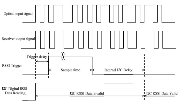
Figure 1 Digital RSSI Timing
Digital Diagnostic Memory Map
The SPET-X53T1-SX3DA transceivers are compliant with the current XFP Multi-Source Agreement (MSA) Specification Rev 4.5. As defined by the XFP MSA, XFP transceivers provide digital diagnostic functions via a 2-wire serial interface, which allows real-time access to the following operating parameters:
Transceiver temperature
Laser bias current
Transmitted optical power
Received optical power
Transceiver supply voltage
It also provides a sophisticated system of alarm and warning flags, which may be used to alert end-users when particular operating parameters are outside of a factory-set normal range.
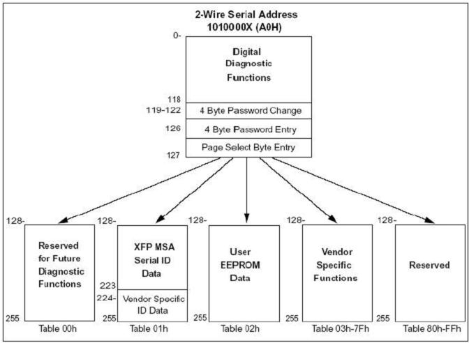
The operating and diagnostics information is monitored and reported by a Digital Diagnostics Transceiver Controller inside the transceiver, which is accessed through the 2-wire serial interface. When the serial protocol is activated, the serial clock signal (SCL pin) is generated by the host. The positive edge clocks data into the XFP transceiver into those segments of its memory map that are not write-protected. The negative edge clocks data from the XFP transceiver. The serial data signal (SDA pin) is bi-directional for serial data transfer. The host uses SDA in conjunction with SCL to mark the start and end of serial protocol activation. The memories are organized as a series of 8-bit data words that can be addressed individually or sequentially. The 2-wire serial interface provides sequential or random access to the 8 bit parameters, addressed from 000h to the maximum address of the memory.
Pin Definitions
Pin Diagram
.jpg)
Pin Descriptions
|
Pin |
Signal Name |
Description |
Notes |
|
1 |
GND |
Module Ground |
Note1 |
|
2 |
VEE5 |
Optional–5.2 Power Supply–Not required |
Note3 |
|
3 |
MOD-DESEL |
Module De-select; When held low allows the module to , respond to 2-wire serial interface commands |
|
|
4 |
INTERRUPT |
Interrupt (bar); Indicates presence of an important condition which can be read over the serial 2-wire interface |
Note2 |
|
5 |
TX_DIS |
Transmitter Disable; Transmitter laser source turned off |
|
|
6 |
VCC5 |
+5 Power Supply |
Note3 |
|
7 |
GND |
Module Ground |
Note1 |
|
8 |
VCC3 |
+3.3V Power Supply |
|
|
9 |
VCC3 |
+3.3V Power Supply |
|
|
10 |
SCL |
Serial 2wire interface clock |
Note2 |
|
11 |
SDA |
Serial 2wire interface data line |
Note2 |
|
12 |
MOD_ABS |
Module Absent; Indicates module is not present. Grounded in the module. |
Note2 |
|
13 |
MOD_NR |
Module Not Ready; |
Note2 |
|
14 |
RX_LOS |
Receiver Loss of Signa lindicator |
Note2 |
|
15 |
GND |
Module Ground |
Note1 |
|
16 |
GND |
Module Ground |
Note1 |
|
17 |
RD- |
Receiver inverted data output |
|
|
18 |
RD+ |
Receiver non-inverted data output |
|
|
19 |
GND |
Module Ground |
Note1 |
|
20 |
VCC2 |
+1.8V Power Supply–No trequired |
Note3 |
|
21 |
RSSI_TRIG |
RSSItriggersignalinputfromthehost |
|
|
22 |
VCC2 |
+1.8V Power Supply–Not required |
Note3 |
|
23 |
GND |
Module Ground |
Note1 |
|
24 |
REFCLK+ |
Reference Clock non-inverted input, AC coupled on the host board–Not required |
Note3 |
|
25 |
REFCLK- |
Reference Clock inverted input, AC coupled on the host board–Not required |
Note3 |
|
26 |
GND |
Module Ground |
Note1 |
|
27 |
GND |
Module Ground |
Note1 |
|
28 |
TD- |
Transmitter inverted data input |
|
|
29 |
TD+ |
Transmitter non-inverted data input |
|
|
30 |
GND |
Module Ground |
Note1 |
Notes:
Plug Seq.: Pin engagement sequence during hot plugging.
1) .Module ground pins GND are isolated from the module case and chassis ground within the module.
2). shall be pulled up with 4.7K-10Kohms to a voltage between 3.15V and 3.45V on the host board.
3). Not connected internally.
Recommended Interface Circuit
TBD
Mechanical Dimensions
TBD
Ordering information
| Part Number | Product Description |
| SPET-X53T1-SX3DA |
Tx 1577nm, Rx 1310nm, 10.3125Gbps/1.25Gbps, 10G/1GBASE-PRX30, 0º C~+70º C, DDM
|
E-mail:sales@sopto.com