
- Sopto Home
-

- SPEU-P351T-SX3DA Asymmetric 10G EPON ONU Transceiver
- Fiber Optic Transceiver Module
- High Speed Cable
- Fiber Optical Cable
- Fiber Optical Patch Cords
- Splitter CWDM DWDM
- PON Solution
- FTTH Box ODF Closure
- PCI-E Network Card
- Network Cables
- Fiber Optical Adapter
- Fiber Optical Attenuator
- Fiber Media Converter
- PDH Multiplexers
- Protocol Converter
- Digital Video Multiplexer
- Fiber Optical Tools
- Compatible
SPEU-P351T-SX3DA Asymmetric 10G EPON ONU Transceiver

SPEU-P351T-SX3DA
Asymmetric 10G EPON ONU Transceiver
Features
Single Fiber Bi-Directional Transceiver with single mode SC receptacle
1310nm burst-mode 1.25G/s transmitter with DFB laser
1577nm continuous-mode 10.3125G/s receiver with APD-TIA
Complies with IEEE P802.3™D3.2 10/1GBASE–PRX30
Digital diagnostic interface compliant with SFF-8472 Rev 9.4 ,
Digital Diagnostic Monitoring (DDM) with external calibration
3.3V Single power supply
LVPECL interface logic level for data input
CML interface logic level for data output
Differential line input/output impedance 100 ohm
LVTTL for burst signal input and LOS detect output
Complies with RoHS directive
Operating case temperature:
Standard: 0 to +70°C
Applications
Asymmetric 10G/1G Ethernet Passive Optical Network ONT
Description
The SPEU-P351T-SX3DA EPON SFP ONU Bi-Directional Transceiver is the high performance module for single fiber communications by using 1310nm 1.25Gbps burst mode transmitter and 1577nm 10.3125Gbps continuous receiver. It is Optical Network Unit (ONU) for IEEE802.3av. The optical transceiver is compliant with the Small Form- Factor Pluggable (SFP) Multi-Source Agreement (MSA).
The transmitter section uses a 1310nm DFB laser diode with automatic power control (APC) function and temperature compensation circuitry to ensure stable extinction ratio overall operating temperature rangeandfullIEC825andCDRHclass1eyesafety.Thereceiverhasahermeticallypackaged APD-TIA(trans-impedanceamplifier)pre-amplifierandalimitingamplifierwithCMLcompatible differentialoutputs.
ThereceiversectionalsoprovidesLVTTLLossofsignaloutput(LOS).Astheinputopticalpoweris decreased,LOSoutputswitchesfromlowtohigh(signallosspoint).Astheinputopticalpoweris increasedfromverylowlevels,LOSoutputwillswitchbackfromhightolow(signaldetectionpoint) thelevelofsignaldetectionpointisatleast0.5dBhigherthanthelevelofsignallosspoint.LVTTL logicinterfacesimplifiesinterfacetoexternalcircuitry.
Absolute Maximum Ratings
Parameter | Symbol | Min. | Max. | Units | Notes |
Storage Temperature | Tst | -40 | +85 | °C | - |
Operating Case Temperature | Tc | 0 | 70 | °C | - |
Operating Humidity | RH | 5 | 90 | % | Non-condensing |
Input Voltage | - | GND | Vcc | V | - |
Power Supply Voltage | Vcc-Vee | 0 | 3.6 | V | - |
Recommended Operating Conditions
Parameter | Symbol | Min | Typical | Max | Unit |
Operating Case Temperature | Tc | 0 | - | +70 | °C |
Power Supply Voltage | Vcc | 3.13 | 3.3 | 3.47 | V |
Power Supply Current | Icc | - | - | 500 | mA |
Optical and Electrical Characteristics
Parameter | Symbol | Min | Typical | Max | Unit | Notes | |||||||||
Transmitter | |||||||||||||||
Tx Data Rate | RT | - | 1.25 | - | Gb/S | - | |||||||||
Centre Wavelength | λc | 1260 | 1310 | 1360 | nm | - | |||||||||
Spectral Width | ∆λ | - | - | 1 | nm | - | |||||||||
Side Mode Suppression Ratio | SMSR | 30 | - | - | dB | - | |||||||||
Average Output Power | Pout | 1 | - | 6 | dBm | 1 | |||||||||
Extinction Ratio | ER | 8 | - | - | dB | - | |||||||||
BurstEnableDelay | Ton | - | - | 32 | ns | Fig.2 | |||||||||
Burst Disable Delay | Toff | - | - | 32 | ns | Fig.2 | |||||||||
Average Launch Power-OFF Transmitter | Poff |
|
| -40 | dBm |
| |||||||||
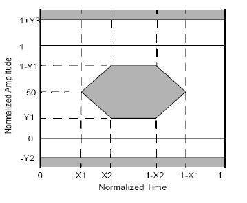
Optical Eye Diagram | Compliant with of IEEE802.3av (Fig.1) transmitter eye mask definition | ||||||||||||||
Optical Rise/Fall Time (20%~80%) | tr/tf |
|
| 260 | ps |
| |||||||||
Data Input Swing Differential | VIN | 200 |
| 1600 | mV | 2 | |||||||||
Input Differential Impedance | ZIN | 90 | 100 | 110 | Ω |
| |||||||||
Burst | Disable |
| 2.0 |
| Vcc | V |
| ||||||||
Enable |
| 0 |
| 0.8 | V |
| |||||||||
TX Fault | Fault |
| 2.0 |
| Vcc | V |
| ||||||||
Normal |
| 0 |
| 0.8 | V |
| |||||||||
Receiver | |||||||||||||||
Rx Data Rate | RR | - | 10.3125 | - | Gb/s |
| |||||||||
Centre Wavelength | λc | 1575 |
| 1580 | nm |
| |||||||||
Receiver Sensitivity | Sen |
|
| -28.5 | dBm | 3 | |||||||||
Stressed receive sensitivity | Sen |
|
| -27 | dBm | 3 | |||||||||
Receiver Overload | Sat | -10 |
|
| dBm | 3 | |||||||||
Damage threshold | - | -9 |
|
|
| 4 | |||||||||
Receiver Reflectance |
|
|
| -12 | dB |
| |||||||||
LOS De-Assert | LOSd | -44 |
|
| dBm |
| |||||||||
LOS Assert | LOSa |
|
| -29 | dBm |
| |||||||||
LOS Hysteresis | - | 0.5 | - | 6 | dB |
| |||||||||
Output Differential Impedance | ZIN | 90 | 100 | 110 | Ω |
| |||||||||
Data Output Swing Differential | Vout | 600 |
| 800 | mV | 5 | |||||||||
LOS Voltage Level | High |
| 2.0 |
| Vcc | V |
| ||||||||
Low |
| 0 |
| 0.8 | V |
| |||||||||
Notes:
1. The optical power is launched into SMF, 1.25Gbps continuous-mode, PRBS27-1.
2. PECL input, internally AC-coupled and terminated.
3. Measured with a PRBS 231-1 test pattern @10312.5Mbps, BER ≤1×10⁻³.
4. Direct ONU-OLT connection may result in damage of the receiver
5. Internally DC-coupled.
Diagnostics
Parameter | Range | Unit | Accuracy | Calibration |
Temperature | 0 to +70 | °C | ±3°C | Internal/External |
Voltage | 3.0 to 3.6 | V | ±3% | Internal/External |
Bias Current | 0 to 100 | mA | ±10% | Internal/External |
TX Power | 1 to 6 | dBm | ±3dB | Internal/External |
RX Power | -29 to -10 | dBm | ±3dB | Internal/External |
Transmitter Burst Mode Timing Characteristics
Definition of Burst Enable Delay (Ton) and Burst Disable Delay (Toff)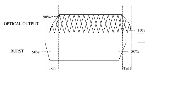
Digital Diagnostic Memory Map
The transceivers provide serial ID memory contents and diagnostic information about the present operating conditions by the 2-wire serial interface (SCL, SDA).The diagnostic information with internal calibration or external calibration all are implemented,including received power monitoring, transmitted power monitoring, bias current monitoring, supply voltage monitoring and temperature monitoring.
The digital diagnostic memory map specific data field defines as following.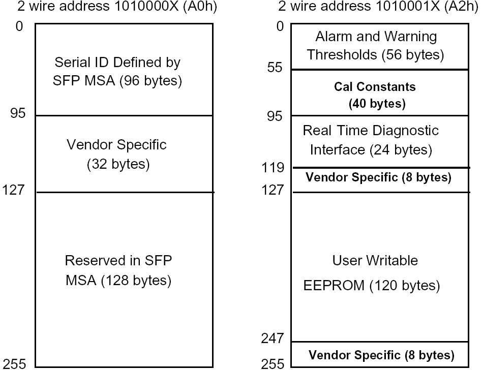
Pin Definitions
Pin Diagram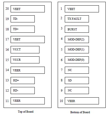
Pin Descriptions
Pin | Signal Name | Description | PlugSeq. | Notes |
1 | VEET | Transmitter Ground | 1 |
|
2 | TX FAULT | Transmitter Fault Indication | 3 | Note1 |
3 | TX DISABLE | Transmitter Disable | 3 | Note2 |
4 | MOD_DEF(2) | SDA Serial Data Signal | 3 | Note3 |
5 | MOD_DEF(1) | SCL Serial Clock Signal | 3 | Note3 |
6 | MOD_DEF(0) | TTL Low | 3 | Note3 |
7 | NC. | Not connect | 3 |
|
8 | LOS | Burst signal detect | 3 | Note4 |
9 |
|
| 3 |
|
10 | VEER | Receiver ground | 1 |
|
11 | VEER | Receiver ground | 1 |
|
12 | RD- | Inv. Received Data Out | 3 | Note5 |
13 | RD+ | Received Data Out | 3 | Note5 |
14 | VEER | Receiver ground | 1 |
|
15 | VCCR | Receiver Power Supply | 2 |
|
16 | VCCT | Transmitter Power Supply | 2 |
|
17 | VEET | Transmitter Ground | 1 |
|
18 | TD+ | Transmit Data In | 3 | Note6 |
19 | TD- | Inv. Transmit Data In | 3 | Note6 |
20 | VEET | Transmitter Ground | 1 |
|
Notes:
Plug Seq.: Pin engagement sequence during hot plugging.
1) TX Fault is an open collector output, which should be pulled up with a 4.7k~10kΩ resistor on the host board to a voltage between 2.0V and Vcc+0.3V. Logic 0 indicates normal operation; Logic 1 indicates a laser fault of some kind. In the low state, the output will be pulled to less than 0.8V.
2) TX Disable is an input that is used to shut down the transmitter optical output. It is pulled up within the module with a 4.7k~10kΩ resistor. Its states are:
Low (0 to 0.8V): Transmitter on
(>0.8V, < 2.0V): Undefined
High (2.0 to 3.465V): Transmitter Disabled
Open: Transmitter Disabled
3) Mod-Def. 0, 1,2. These are the module definition pins. They should be pulled up with a 4.7k~10kΩ resistor on the host board. The pull-up voltage shall be VccT or VccR.
Mod-Def. 0 is grounded by the module to indicate that the module is present
Mod-Def. 1 is the clock line of two wire serial interface for serial ID
Mod-Def. 2 is the data line of two wire serial interface for serial ID
4) LOS (Loss of Signal) is an open collector/drain output, which should be pulled up with a 4.7K – 10KΩ resistor. Pull up voltage between 2.0V and VccT, R+0.3V. When high, this output indicates the received optical power is below the worst-case receiver sensitivity (as defined by the standard in use). Low indicates normal operation. In the low state, the output will be pulled to < 0.8V.
5) RD-/+: These are the differential receiver outputs. They are internally DC-coupled 100 differential lines which should be terminated with 100Ω (differential) at the user SERDES.
6) TD-/+: These are the differential transmitter inputs. They are internally AC-coupled, differential lines with 100Ω differential termination inside the module.
Recommended Application Circuit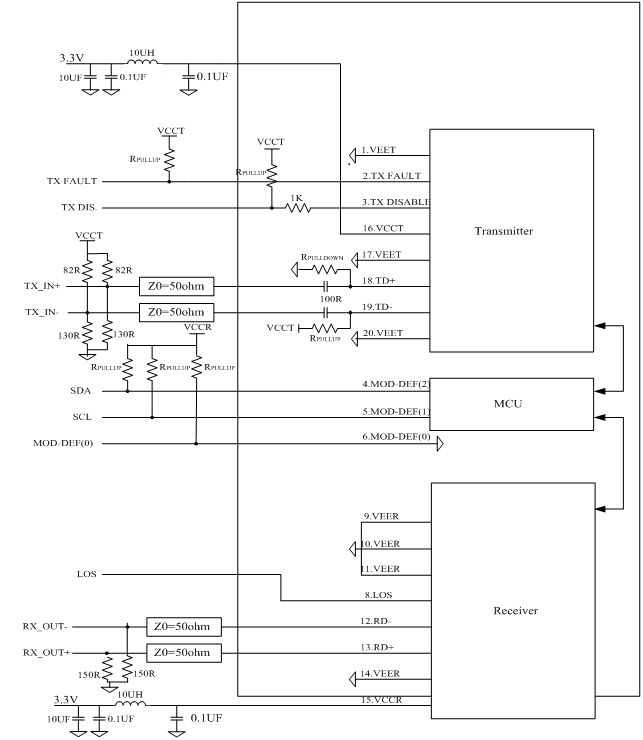
Mechanical Dimensions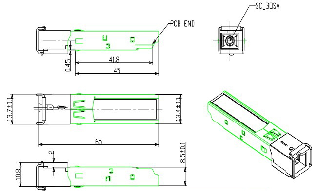
Orderinginformation
| Part Number | Product Description |
| SPEU-P351T-SX3DA | Tx 1310nm, Rx 1577nm, 1.25Gbps/10.3125Gbps, 10/1GBASE-PRX30, 0º C~+70º C,DDM |
E-mail:sales@sopto.com