- Sopto Home
-

- 10G XENPAK transceiver CWDM SPT-KC(47-61)TG-40D
- Fiber Optic Transceiver Module
- High Speed Cable
- Fiber Optical Cable
- Fiber Optical Patch Cords
- Splitter CWDM DWDM
- PON Solution
- FTTH Box ODF Closure
- PCI-E Network Card
- Network Cables
- Fiber Optical Adapter
- Fiber Optical Attenuator
- Fiber Media Converter
- PDH Multiplexers
- Protocol Converter
- Digital Video Multiplexer
- Fiber Optical Tools
- Compatible
10G XENPAK transceiver CWDM SPT-KC(47-61)TG-40D

TG-40D-1.jpg) Features
Features
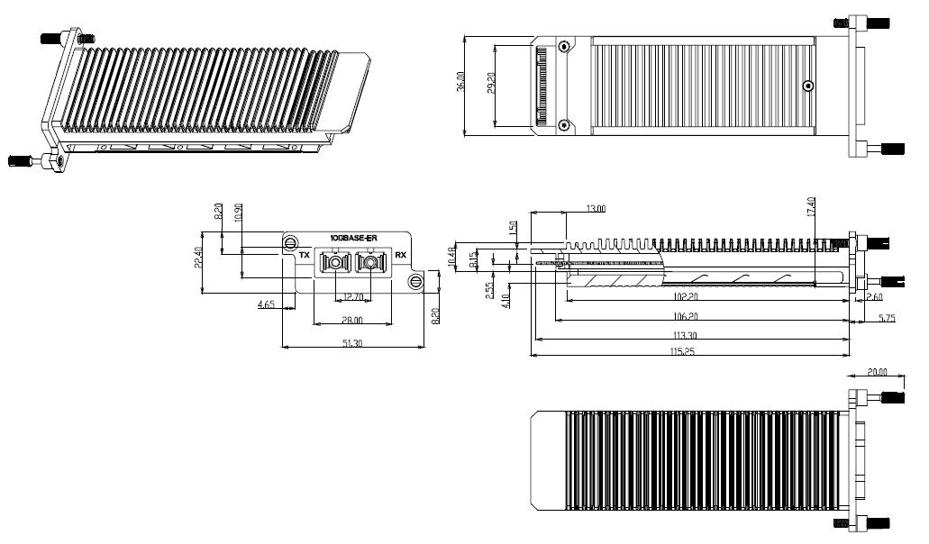
- XENPAK MSA Compliant
- 70-PIN connector
- SC duplex receptacle package
- Wavelength selectable to ITU-T standards covering
- CWDM grid wavelengths
- Cooled EA-DFB/PIN-PD
- Power supply: +5.0 V, +3.3 V, APS:+1.2 V
- Power Dissipation 4W Maximum
- 0ºC to 70ºC Operating Case Temperature
- Digital Diagnostic Monitoring
- Management and control with MDIO 2-wire bus
- XAUI electrical interface 4 x 3.125 Gb/s Ethernet
- ≤40km ER(Extended Range)10GBE
- RoHS compliant and lead free
Applications
- 10 Gb/s Ethernet transmission systems
Absolute Maximum Ratings
|
Parameter |
Symbol |
Min |
Max |
Unit |
|
Supply Voltage+5V |
Vcc5 |
|
6.0 |
V |
|
Supply Voltage_3.3V |
Vcc3 |
|
4 |
V |
|
Supply Voltage APS |
Vaps |
|
2 |
V |
|
Storage Temperature |
Tst |
-20 |
85 |
ºC |
|
Optical Input Received Power |
PIN |
- |
-1 |
dBm |
Operating Conditions
|
Parameter |
Symbol |
Min |
Typical |
Max |
Unit |
|
Operating Case temperature |
Tca |
0 |
- |
70 |
ºC |
|
Supply Voltage+5V |
Vcc5 |
4.75 |
5 |
5.25 |
V |
|
Supply Current+5V |
Icc5 |
|
|
500 |
mA |
|
Supply Voltage_3.3V |
VCC3 |
3.14 |
3.3 |
3.47 |
V |
|
Supply Current+3.3V |
Icc3 |
|
|
1000 |
mA |
|
Supply Voltage APS |
Vaps |
1.14 |
1.2 |
1.26 |
V |
|
Supply Current APS |
Iaps |
|
|
1100 |
mA |
|
Module Power Dissipation |
Pm |
- |
|
4 |
W |
Transmitter Specifications – Optical
|
Parameter |
Symbol |
Min |
Typical |
Max |
Unit |
|
Center Wavelength |
ëc |
1464.5 |
|
1617.5 |
nm |
|
Center wavelength stability |
ÄëD |
−6.5 |
ëc |
6.5 |
nm |
|
Optical Transmit Power |
Po |
-1 |
|
2 |
dBm |
|
Optical Transmit Power (disabled) |
Ptx-dis |
- |
- |
-40 |
dBm |
|
Extinction Ratio |
ER |
9 |
|
- |
dB |
|
Side Mode Suppression Ratio |
SMSR |
30 |
- |
- |
dB |
|
Eye Mask |
IEEE 802.3ae Compliant |
||||
Transmitter Specifications – Electrical
|
Parameter |
Symbol |
Min |
Typical |
Max |
Unit |
|
Data Rate (TXLINE0-3) |
TX-xaui |
- |
3125 |
- |
Mbps |
|
Differential impedance |
Zo |
80 |
100 |
120 |
Ω |
|
Differential Input Amplitude |
Vin P-P |
160 |
- |
2000 |
mVpp |
|
Input Rise/Fall |
TR / TF |
60 |
- |
130 |
ps |
|
Differential Impedance of Zin |
Zin |
- |
100 |
- |
ohm |
Receiver Specifications – Optical
|
Parameter |
Symbol |
Min |
Typical |
Max |
Unit |
|
||||||
|
Received power |
Rpo |
-15 |
- |
-3 |
dBm |
|
||||||
|
Maximum Input Power |
RX-overload |
-3 |
- |
- |
dBm |
|
||||||
|
|
Input Operating Wavelength |
λ |
1260 |
- |
1565 |
nm |
||||||
|
|
Reflectance |
Rrx |
- |
- |
-27 |
dB |
||||||
Receiver Specifications – Electrical
|
Parameter |
Symbol |
Min |
Typical |
Max |
Unit |
|
Data Rate (TXLINE0-3) |
RX-xaui |
|
3125 |
|
Mbps |
|
Supply Voltage |
VccRX |
3.13 |
3.3 |
3.47 |
V |
|
Differential Output Amplitude |
Vout P-P |
800 |
- |
1600 |
mV |
|
Rise/Fall Time |
Tr / Tf |
50 |
- |
90 |
ps |
|
Differential Impedance of Zout |
Zout |
- |
100 |
- |
ohm |
Signal Specifications – Electrical
|
Parameter |
Symbol |
Min |
Typ |
Max |
Units |
|
1.2 V CMOS |
|||||
|
Input High Voltage |
VIL(MAX) |
- |
- |
0.36 |
V |
|
Input Low Voltage |
VIH(MIN) |
0.84 |
- |
1.25 |
V |
|
Capacitance |
|
- |
- |
320 |
pF |
|
Pull Up Resistance |
Rpull |
10k |
- |
22k |
ohm |
|
MDIO I/O |
|||||
|
Output Low Voltage |
VOL |
-0.3 |
- |
0.2 |
V |
|
Output Low Current |
IOL |
- |
- |
4 |
mA |
|
Input High Voltage |
VIH |
0.84 |
- |
1.5 |
V |
|
Input Low Voltage |
VIL |
-0.3 |
- |
0.36 |
V |
|
Pull-up Supply Voltage |
VPULL |
1.14 |
1.2 |
1.26 |
|
|
Input Capacitance |
CIN |
- |
- |
10 |
Pf |
|
Load Capacitance |
CLOD |
- |
- |
470 |
Pf |
|
External Pull-up Resistance |
EPULL |
200 |
- |
- |
Ohm |
Table 3: Digital Diagnostic Monitoring Accuracy
|
Parameter |
Accuracy |
Unit |
|
Temperature |
± 5 |
℃ |
|
Bias Current |
± 10 |
% |
|
TX Power |
± 3 |
DBm |
|
RX Power |
± 3 |
DBm |
Pin Definitions
|
Pin No |
Name |
Dir |
Function |
Notes |
|
1 |
GND |
|
Electrical Ground |
1 |
|
2 |
GND |
|
Electrical Ground |
1 |
|
3 |
GND |
|
Electrical Ground |
1 |
|
4 |
5.0V |
|
Power |
2 |
|
5 |
3.3V |
|
Power |
2 |
|
6 |
3.3V |
|
Power |
2 |
|
7 |
APS =1.2V |
|
Adaptive Power Supply |
2 |
|
8 |
APS =1.2V |
|
Adaptive Power Supply |
2 |
|
9 |
LASI |
|
Open Drain Compatible 10K-22K pull up on host. Logic High: Normal Operation Logic Low: LASI Asserted |
4 |
|
10 |
RESET |
I |
Open Drain compatible. 10-22K pull-up on transceiver Logic high = Normal operation Logic low = Reset Minimum reset assert time 1 ms |
4 |
|
11 |
VEND SPECIFIC |
|
Vendor Specific Pin. Leave unconnected when not in use. |
8 |
|
12 |
TX ON/OFF |
I |
Open Drain compatible. 10-22K pull-up on transceiver Logic high = Transmitter On (capable) Logic low = Transmitter Off (always) |
4 |
|
13 |
RESERVED |
|
Reserved |
4 |
|
14 |
MOD DETECT |
O |
Pulled low inside module through 1k |
|
|
15 |
VEND SPECIFIC |
|
Vendor Specific Pin. Leave unconnected when not in use. |
8 |
|
16 |
VEND SPECIFIC |
|
Vendor Specific Pin. Leave unconnected when not in use. |
8 |
|
17 |
MDIO |
I/O |
Management Data IO |
4, 5 |
|
18 |
MDC |
I |
Management Data Clock |
4, 5 |
|
19 |
PRTAD4 |
I |
Port Address Bit 4 (Low = 0) |
4 |
|
20 |
PRTAD3 |
I |
Port Address Bit 3 (Low = 0) |
4 |
|
21 |
PRTAD2 |
I |
Port Address Bit 2 (Low = 0) |
4 |
|
22 |
PRTAD1 |
I |
Port Address Bit 1 (Low = 0) |
4 |
|
23 |
PRTAD0 |
I |
Port Address Bit 0 (Low = 0) |
4 |
|
24 |
VEND SPECIFIC |
|
Vendor Specific Pin. Leave unconnected when not in use. |
8 |
|
25 |
APS SET |
|
Feedback input for APS |
|
|
26 |
RESERVED |
|
Reserved for Avalanche Photodiode use. |
8 |
|
27 |
APS SENSE |
|
APS Sense Connection |
|
|
28 |
APS =1.2V |
|
Adaptive Power Supply |
2 |
|
29 |
APS =1.2V |
|
Adaptive Power Supply |
2 |
|
30 |
3.3V |
|
Power |
2 |
|
31 |
3.3V |
|
Power |
2 |
|
32 |
5.0V |
|
Power |
2 |
|
33 |
GND |
|
Electrical Ground |
1 |
|
34 |
GND |
|
Electrical Ground |
1 |
|
35 |
GND |
|
Electrical Ground |
1 |
|
36 |
GND |
|
Electrical Ground |
1 |
|
37 |
GND |
|
Electrical Ground |
1 |
|
38 |
RESERVED |
|
Reserved |
|
|
39 |
RESERVED |
|
Reserved |
|
|
40 |
GND |
|
Electrical Ground |
1 |
|
41 |
RX LANE0+ |
O |
Module XAUI Output Lane 0+ |
7 |
|
42 |
RX LANE0- |
O |
Module XAUI Output Lane 0- |
7 |
|
43 |
GND |
|
Electrical Ground |
1 |
|
44 |
RX LANE1+ |
O |
Module XAUI Output Lane 1+ |
7 |
|
45 |
RX LANE1- |
O |
Module XAUI Output Lane 1- |
7 |
|
46 |
GND |
|
Electrical Ground |
1 |
|
47 |
RX LANE2+ |
O |
Module XAUI Output Lane 2+ |
7 |
|
48 |
RX LANE2- |
O |
Module XAUI Output Lane 2- |
7 |
|
49 |
GND |
|
Electrical Ground |
1 |
|
50 |
RX LANE3+ |
O |
Module XAUI Output Lane 3+ |
7 |
|
51 |
RX LANE3- |
O |
Module XAUI Output Lane 3- |
7 |
|
52 |
GND |
|
Electrical Ground |
1 |
|
53 |
GND |
|
Electrical Ground |
1 |
|
54 |
GND |
|
Electrical Ground |
1 |
|
55 |
TX LANE0+ |
I |
Module XAUI Input Lane 0+ |
7 |
|
56 |
TX LANE0- |
I |
Module XAUI Input Lane 0- |
7 |
|
57 |
GND |
|
Electrical Ground |
1 |
|
58 |
TX LANE1+ |
I |
Module XAUI Input Lane 1+ |
7 |
|
59 |
TX LANE1- |
I |
Module XAUI Input Lane 1- |
7 |
|
60 |
GND |
|
Electrical Ground |
1 |
|
61 |
TX LANE2+ |
I |
Module XAUI Input Lane 2+ |
7 |
|
62 |
TX LANE2- |
I |
Module XAUI Input Lane 2- |
7 |
|
63 |
GND |
|
Electrical Ground |
1 |
|
64 |
TX LANE3+ |
I |
Module XAUI Input Lane 3+ |
7 |
|
65 |
TX LANE3- |
I |
Module XAUI Input Lane 3- |
7 |
|
66 |
GND |
|
Electrical Ground |
1 |
|
67 |
RESERVED |
|
Reserved |
|
|
68 |
RESERVED |
|
Reserved |
|
|
69 |
GND |
|
Electrical Ground |
1 |
|
70 |
GND |
|
Electrical Ground |
1 |
Notes:
1) Ground connections are common for TX and RX.
2) All connector contacts are rated at 0.5A nominal.
4) 1.2V CMOS compatible.
5) MDIO and MDC timing must comply with IEEE802.3ae, Clause 45.3
7) XAUI output characteristics should comply with IEEE802.3ae Clause 47.
8) Transceivers will be MSA compliant when no signals are present on the vendor specific pins.
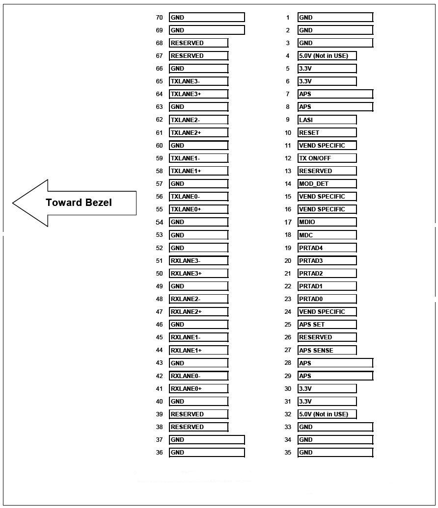
Figure1.Electrical Pin-out Details
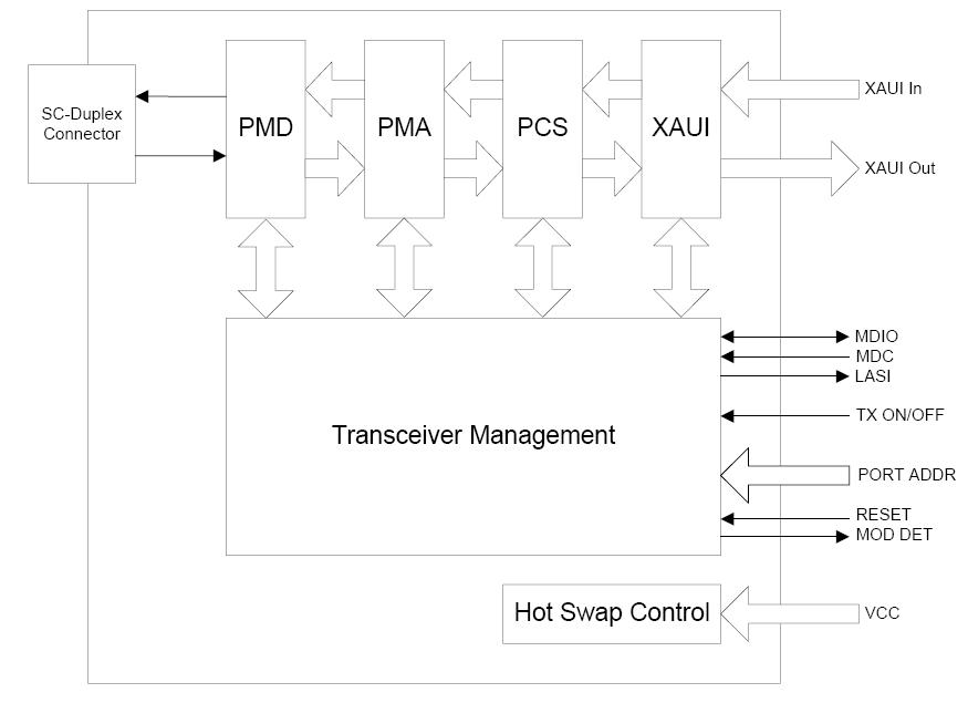
Figure2. Functional Diagram of Typical XENPAK Style Transceiver