
- Sopto Home
-

- 125M 1310nm 2km SGMII SFP Fiber Optic Transceiver Module SPT-PH3102-02D
- Fiber Optic Transceiver Module
- High Speed Cable
- Fiber Optical Cable
- Fiber Optical Patch Cords
- Splitter CWDM DWDM
- PON Solution
- FTTH Box ODF Closure
- PCI-E Network Card
- Network Cables
- Fiber Optical Adapter
- Fiber Optical Attenuator
- Fiber Media Converter
- PDH Multiplexers
- Protocol Converter
- Digital Video Multiplexer
- Fiber Optical Tools
- Compatible
125M 1310nm 2km SGMII SFP Fiber Optic Transceiver Module SPT-PH3102-02D

SPT-PH3102-02D
SFP 100Base-FX 1310nm 2km Reach
Features
- Build-in PHY supporting SGMII Interface
- 100BASE-FX operation
- 1310nm FP laser and PIN photo-detector
- 2km transmission with MMF
- Standard serial ID information Compatible with SFP MSA
- SFP MSA package with duplex LC connector
- With Spring-Latch for high density application
- Very low EMI and excellent ESD protection
- +3.3V single power supply
- Operating case temperature: 0 to +70°C
Applications
- Switch to Switch interface
- Switched backplane applications
- Router/Server interface
- Gigabit Ethernet To Fast Ethernet
- Other optical transmission systems
Standard
- Compatible with SFP MSA
- Compatible with IEEE 802.3ah-2004
Description
The SFP transceiver is high performance, cost effective modules. It is designed for100BASE-FX Applications of 2km with MMF. The transceiver consists of two sections: The standard SFP part and thePHY part built with SGMII interface. The optical output can be disabled by a TTL logic high-level input of Tx Disable, and the system also can disable the module via I2C. Tx Fault is provided to indicate that degradation of the laser. Loss of signal (LOS) output is provided to indicate the loss of an input optical signal of receiver or the link status with partner. The system can also get the LOS(or Link)/Disable/Fault information via I2C register access. The standard serial ID information Compatible with SFP MSA describes the transceiver’s capabilities, standard interfaces, manufacturer and other information. The host equipment can access this information via the 2-wire serial CMOS EEPROM protocol. For further information, please refer to SFP Multi-Source Agreement (MSA).
Absolute Maximum Ratings
Stress in excess of the maximum absolute ratings can cause permanent damage to the module
|
Parameter |
Symbol |
Min |
Max |
Unit |
|
Maximum Supply Voltage |
Vcc |
-0.5 |
3.6 |
V |
|
Storage Temperature |
TS |
-40 |
100 |
℃ |
|
Relative Humidity |
RH |
0 |
85 |
% |
Recommended Operating Conditions
|
Parameter |
Symbol |
Min |
Typical |
Max |
Unit |
|
Operating Case Temperature |
TC |
0 |
|
70 |
℃ |
|
Power Supply Voltage |
VCC |
3.1 |
3.3 |
3.5 |
V |
|
Power Supply Current |
Icc |
|
|
420 |
mA |
|
Data Rate |
|
|
125 |
|
Mbps |
Optical and Electrical Characteristics
|
Parameter |
Symbol |
Min. |
Typical |
Max. |
Unit |
Notes |
||||||||||
|
Transmitter |
||||||||||||||||
|
Centre Wavelength |
λC |
1261 |
1310 |
1360 |
nm |
|
||||||||||
|
Average Output Power |
P0ut |
-20 |
|
-14 |
dBm |
2 |
||||||||||
|
Spectral Width (RMS) |
σ |
|
|
7.7 |
nm |
2 |
||||||||||
|
Extinction Ratio |
EX |
10 |
|
17 |
dB |
|
||||||||||
|
Rise/Fall Time |
Tr/Tf |
|
|
3 |
ns |
3 |
||||||||||
|
|
Output Optical Eye |
Compatible with IEEE 802.3ah-2004 |
4 |
|||||||||||||
|
|
Data Input Swing Differential (SGMII Series interface) |
VIN |
200 |
|
2100 |
mV |
5 |
|||||||||
|
|
Input Differential Impedance |
ZIN |
80 |
100 |
120 |
Ω |
|
|||||||||
|
|
TX Disable |
Disable |
|
2.0 |
|
Vcc |
V |
|
||||||||
|
|
Enable |
|
0 |
|
0.8 |
V |
|
|||||||||
|
|
TX Fault |
Fault |
|
2.0 |
|
Vcc+0.3 |
V |
|
||||||||
|
|
Normal |
|
0 |
|
0.8 |
V |
|
|||||||||
|
|
Receiver |
|||||||||||||||
|
|
Centre Wavelength |
λC |
1260 |
|
1570 |
nm |
|
|||||||||
|
|
Receiver Sensitivity |
|
|
|
-31 |
dBm |
6 |
|||||||||
|
|
Receiver Overload |
|
-10 |
|
|
dBm |
6 |
|||||||||
|
|
LOS De-Assert |
LOSD |
|
|
-32.5 |
dBm |
|
|||||||||
|
|
LOS Assert |
LOSA |
-45 |
|
|
dBm |
|
|||||||||
|
|
LOS Hysteresis |
|
1 |
|
4.5 |
dB |
|
|||||||||
|
|
Total Jitter (SGMII Series Interface) |
Tj |
|
|
0.43 |
UI |
|
|||||||||
|
|
Data Output Swing Differential |
VOUT |
370 |
|
2000 |
mV |
5 |
|||||||||
|
|
LOS |
High |
|
2.0 |
|
Vcc+0.3 |
V |
|
||||||||
|
|
Low |
|
0 |
|
0.8 |
V |
|
|||||||||
Notes:
2. The optical power is launched into MMF 50/125um.
3. Unfiltered, measured with 4B/5B code for 125Mbps
4. Measured with 4B/5B code for 125Mbps.
5. PECL logic, internally AC coupled.
6. Measured with 4B/5B code for 125Mbps, worst-case extinction ratio, BER ≤1×10⁻¹⁰
Diagnostics
|
Parameter |
Range |
Unit |
Accuracy |
Calibration |
|
Temperature |
0 to 70 |
℃ |
±3℃ |
Internal / External |
|
Voltage |
0 to VCC |
V |
±3% |
Internal / External |
|
Bias Current |
0 to 100 |
mA |
±10% |
Internal / External |
|
TX Power |
-12 to -18 |
dBm |
±3 dB |
Internal / External |
|
RX Power |
-30 to -12 |
dBm |
±3 dB |
Internal / External |
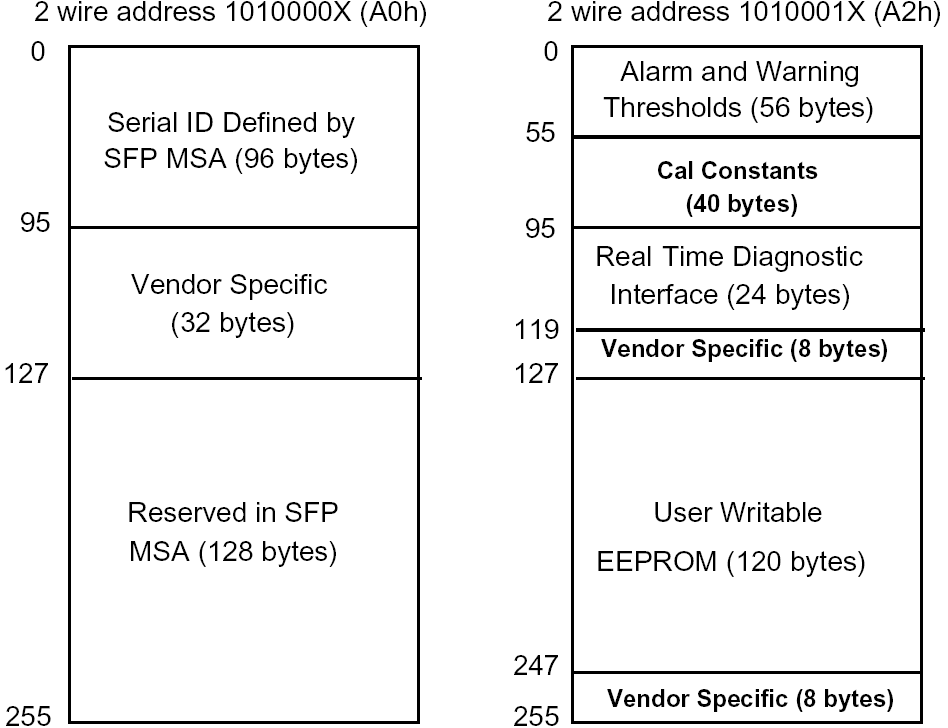
EEPROM Section
The optical transceiver contains an EEPROM. It provides access to sophisticated identification information that describes the transceiver’s capabilities, standard interfaces, manufacturer, and other information.
The serial interface uses the 2-wire serial CMOS EEPROM protocol defined for the MCU family of components. When the serial protocol is activated, the host generates the serial clock signal (SCL, Mod Def 1). The positive edge clocks data into those segments of the EEPROM that are not write-protected within the SFP transceiver. The negative edge clocks data from the SFP transceiver. The serial data signal (SDA, Mod Def 2) is bi-directional for serial data transfer. The hostuses SDA in conjunction with SCL to mark the start and end of serial protocol activation. The memories are organized as a seriesof 8-bit data words that can be addressed individually or sequentially.
The Module provides diagnostic information about the present operating conditions. The transceiver generates this diagnosticdata by digitization of internal analog signals. Calibration and alarm/warning threshold data is written during device manufacture. Received power monitoring, transmitted power monitoring, bias current monitoring, supply voltage monitoring and temperature monitoring all are implemented. The diagnostic data are raw A/D values and must be converted to real world units usingcalibration constants stored in EEPROM locations 56 – 95 at wire serial bus address A2h. The digital diagnostic memory map specific data field define as following.
Pin Definitions
Pin Diagram
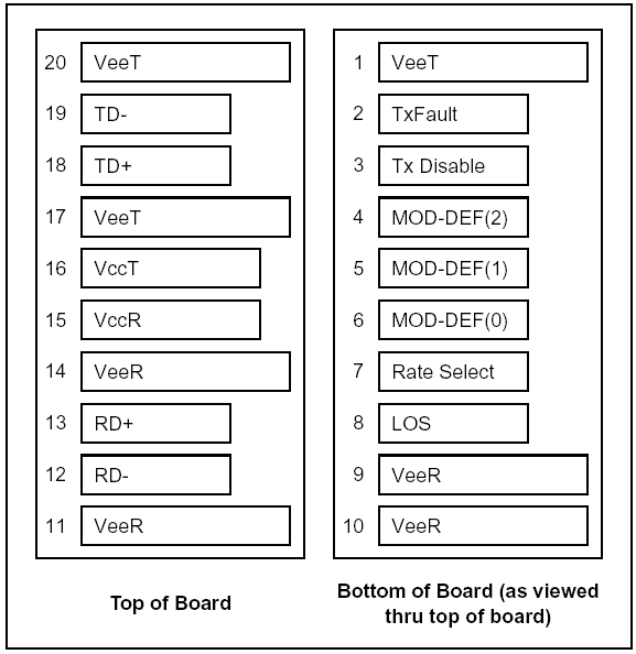
Pin Descriptions
|
Pin |
Signal Name |
Description |
Plug Seq. |
Notes |
|
1 |
VEET |
Transmitter Ground |
1 |
|
|
2 |
TX FAULT |
Transmitter Fault Indication |
3 |
Note1 |
|
3 |
TX DISABLE |
Transmitter Disable |
3 |
Note2 |
|
4 |
MOD_DEF(2) |
SDA Serial Data Signal |
3 |
Note3 |
|
5 |
MOD_DEF(1) |
SCL Serial Clock Signal |
3 |
Note3 |
|
6 |
MOD_DEF(0) |
TTL Low |
3 |
Note3 |
|
7 |
Rate Select |
Not Connected |
3 |
|
|
8 |
LOS |
Loss of Signal |
3 |
Note 4 |
|
9 |
VEER |
Receiver ground |
1 |
|
|
10 |
VEER |
Receiver ground |
1 |
|
|
11 |
VEER |
Receiver ground |
1 |
|
|
12 |
RX- |
Inv. Received Data Out |
3 |
Note 5 |
|
13 |
RX+ |
Received Data Out |
3 |
Note 5 |
|
14 |
VEER |
Receiver ground |
1 |
|
|
15 |
VCCR |
Receiver Power Supply |
2 |
|
|
16 |
VCCT |
Transmitter Power Supply |
2 |
|
|
17 |
VEET |
Transmitter Ground |
1 |
|
|
18 |
TX+ |
Transmit Data In |
3 |
Note 6 |
|
19 |
TX- |
Inv. Transmit Data In |
3 |
Note 6 |
|
20 |
VEET |
Transmitter Ground |
1 |
|
Notes:
Plug Seq.: Pin engagement sequence during hot plugging.
1) TX Fault is an open collector output, which should be pulled up with a 4.7k~10kΩ resistor on the host board to a voltage between 2.0V and Vcc+0.3V. Logic 0 indicates normal operation; Logic 1 indicates a laser fault of some kind. In the low state, the output will be pulled to less than 0.8V.
2) TX Disable is an input that is used to shut down the transmitter optical output. It is pulled up within the module with a
4.7k~10kΩ resistor. Its states are:
Low (0 to 0.8V): Transmitter on
(>0.8V, < 2.0V): Undefined
High (2.0 to 3.465V): Transmitter Disabled
Open: Transmitter Disabled
3) Mod-Def 0,1,2. These are the module definition pins. They should be pulled up with a 4.7k~10kΩ resistor on the host board. The pull-up voltage shall be VccT or VccR.
Mod-Def 0 is grounded by the module to indicate that the module is present
Mod-Def 1 is the clock line of two wire serial interface for serial ID Mod-Def 2 is the data line of two wire serial interface for serial ID
4) LOS is an open collector output, which should be pulled up with a 4.7k~10kΩ resistor. Pull up voltage between 2.0V and
Vcc+0.3V. Logic 1 indicates loss of signal; Logic 0 indicates normal operation. In the low state, the output will be pulled to less than 0.8V.
5) RD-/+: These are the differential receiver outputs. They are internally AC-coupled 100 differential lines which should be
terminated with 100Ω (differential) at the user SERDES.
6) TD-/+: These are the differential transmitter inputs. They are internally AC-coupled, differential lines with 100Ω differential termination inside the module.
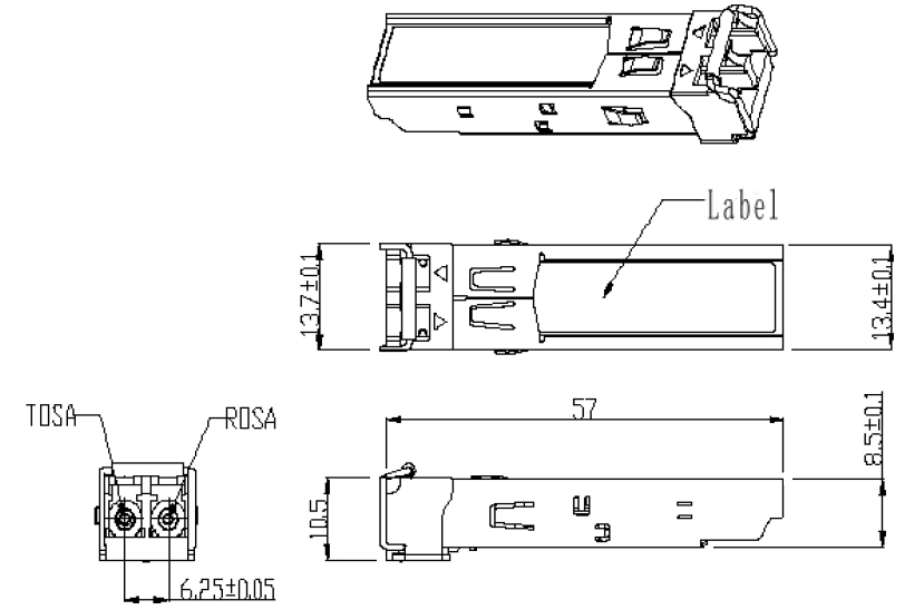
Mechanical Dimensions
Ordering information
|
Part Number |
Product Description |
|
SPT-PH3102-02 |
1310nm,2km,125Mbps, 0ºC ~ +70ºC |
|
SPT-PH3102-02D |
1310nm,2km,125Mbps, 0ºC ~ +70ºC, With Digital Diagnostic Monitoring |
E-mail: sales@sopto.com
Web : http://www.sopto.com