
- Sopto Home
-

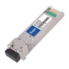
- 8.5G 850nm 150m SFP+ Channel Optical Transceiver SPT-SFP-8G-SR
- Fiber Optic Transceiver Module
- High Speed Cable
- Fiber Optical Cable
- Fiber Optical Patch Cords
- Splitter CWDM DWDM
- PON Solution
- FTTH Box ODF Closure
- PCI-E Network Card
- Network Cables
- Fiber Optical Adapter
- Fiber Optical Attenuator
- Fiber Media Converter
- PDH Multiplexers
- Protocol Converter
- Digital Video Multiplexer
- Fiber Optical Tools
- Compatible
8.5G 850nm 150m SFP+ Channel Optical Transceiver SPT-SFP-8G-SR

Features
- Up to 8.5Gb/s bi-directional data links
- Hot Pluggable SFP+ footprint
- 850nm VCSEL transmitter, PIN photo-detector
- Transmission distance up to 150m OM3 MMF
- Digital Status monitoring Interface
- Duplex LC connector
- RoHS compliant and Lead Free
- Metal enclosure for lower EMI
- Single 3.3V power supply
- Operating case temperature: 0 to 70℃
- Compliant with FC-PI-4 800-Mx-SN-I, SFF-8431 , SFF-8432 and SFF-8472
Applications
- Tri Rate 1.0625/2.125/4.25/8.5Gbs Fiber Channel
Product description
These transceivers are designed for using in Fiber Channel links up to 8.5 GB/s data rate over multimode fiber and compliant to SFI electrical specifications. The transmitter input and receiver output impedance is 100 Ohms differential. Data lines are internally AC coupled. The module provides differential termination and reduce differential to common mode conversion for quality signal termination and low EMI.
Pin definition
The SFP+ modules are hot-pluggable. Hot pluggable refers to plugging in or unplugging a module while the host board is powered. The SFP+ host connector is a 0.8 mm pitch 20 position right angle improved connector specified by SFF-8083, or stacked connector with equivalent with equivalent electrical performance. Host PCB contact assignment is shown in Figure 2 and contact definitions are given in Table 2.SFP+ module contacts mates with the host in the order of ground, power, followed by signal as illustrated by Figure 3 and the contact sequence order listed in Table 2.
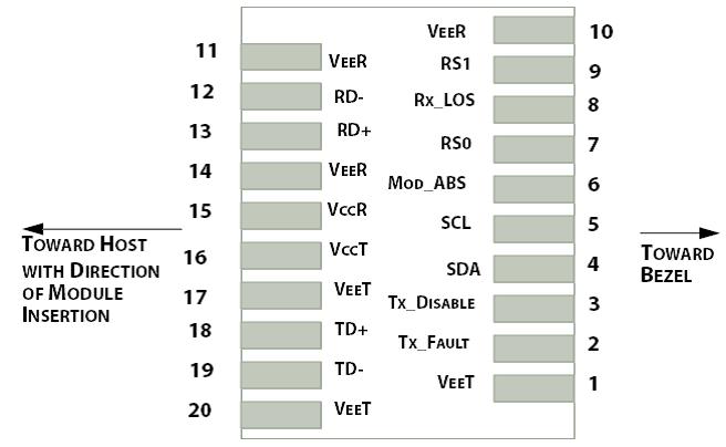
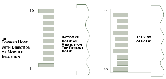
Figure 3: Module Contact Assignment
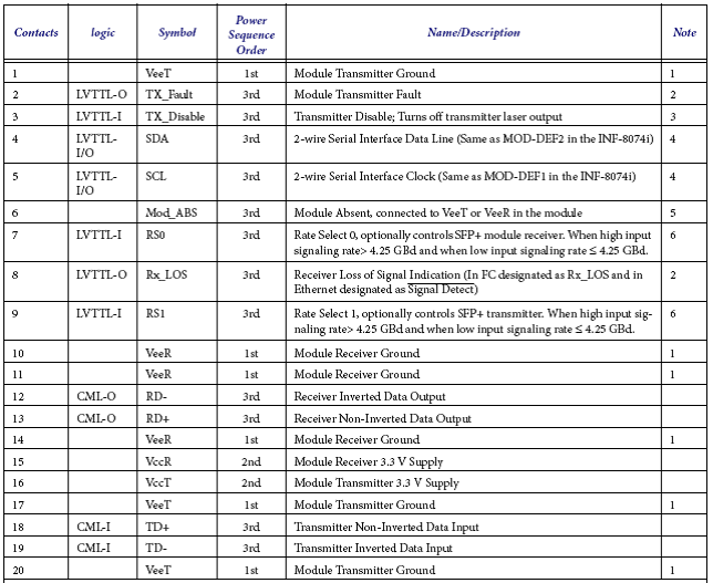
Table 2: SFP+ Module PIN Definition
Absolute maximum rating
These values represent the damage threshold of the module. Stress in excess of any of the individual Absolute Maximum Ratings can cause immediate catastrophic damage to the module even if all other parameters are within Recommended Operating Conditions.
|
Parameters |
Symbol |
Min. |
Max. |
Unit |
|
Power Supply Voltage |
VCC |
0 |
+3.6 |
V |
|
Storage Temperature |
Tc |
-40 |
+85 |
°C |
|
Operating Case Temperature |
Tc |
0 |
+70 |
°C |
|
Relative Humidity |
RH |
5 |
95 |
% |
Recommended operating environment
Recommended Operating Environment specifies parameters for which the electrical and optical characteristics hold unless otherwise noted.
|
Parameter |
Symbol |
Min. |
Typical |
Max |
Unit |
|
Power Supply Voltage |
VCC |
3.135 |
3.300 |
3.465 |
V |
|
Operating Case Temperature |
TC |
0 |
25 |
70 |
°C |
LOW Speed Characteristics
|
Parameter |
Symbol |
Min. |
Typical |
Max |
Unit |
|
Power Consumption |
|
|
0.6 |
0.8 |
W |
|
TX_Fault,RX_LOS |
VOL |
0 |
|
0.4 |
V |
|
VOH |
Host_Vcc-0.5 |
|
Host_Vcc+0.3 |
V |
|
|
TX_DIS |
VIL |
-0.3 |
|
0.8 |
V |
|
VIH |
2.0 |
|
VCCT+0.3 |
V |
|
|
RS0,RS1 |
VIL |
-0.3 |
|
0.8 |
V |
|
VIH |
2.0 |
|
VCCT+0.3 |
V |
Transmitter Input Characteristics
|
Parameter |
Conditions |
Symbol |
Min. |
Typical |
Max |
Unit |
|
Nominal Data Rate |
|
VID |
2.125 |
8.5 |
8.5 |
Gbd |
|
Reference Differential Input Impedance |
|
Zd |
|
100 |
|
Ω |
|
Input AC Common Mode Input Voltage |
|
|
|
0 |
25 |
mV (RMS) |
|
Differential Input Voltage Swing |
|
VID |
150 |
|
900 |
mV |
|
Differential Input S-parameter |
0.01-3.9GHz |
SDD11 |
|
|
-10 |
dB |
|
3.9-8.5GHz |
|
Note1 |
|
Note1 |
|
|
|
Differential to Common Mode Conversion Note 2 |
0.01-8.5GHz |
SCD11 |
|
|
-10 |
dB |
|
Data Dependant Jitter |
|
DDJ |
|
|
0.1 |
UI(p-p) |
|
Total Jitter |
|
TJ |
|
|
0.28 |
UI(P-P) |
|
Uncorrelated Jitter |
|
UJ |
|
|
0.023 |
RMS |
1) Differential Return Loss given by equation SDD11(dB) = -8+13.33 Log10(f/5.5), with f in GHz
2) Common mode reference impedance is 25Ω. Differential to common mode conversion relates to generation of EMI
Receiver Output Characteristics
|
Parameter |
Conditions |
Symbol |
Min. |
Typical |
Max |
Unit |
|
Nominal Data Rate |
|
VID |
2.125 |
8.5 |
8.5 |
Gbd |
|
Reference Differential Input Impedance |
|
Zd |
|
100 |
|
Ω |
|
Termination Mismatch |
|
ΔZd
|
|
|
5 |
% |
|
Output AC Common Mode Input Voltage |
|
|
|
|
15 |
mV (RMS) |
|
Output Rise and Fall time |
20% to 80% |
tRH, tFH
|
|
|
35 |
ps |
|
Differential Input Voltage Swing |
Zload=100ohm |
VOD |
350 |
|
800 |
mV |
|
Differential Input S-parameter |
0.01-3.9GHz |
SDD22 |
|
|
-10 |
dB |
|
3.9-8.5GHz |
|
Note1 |
|
Note1 |
|
|
|
Differential to Common Mode Conversion Note2 |
0.01-6.5GHz |
SCCD22 |
|
|
-7 |
dB |
|
Differential to Common Mode Conversion Note2 |
6.5-8.5GHz |
SCCD22 |
|
|
-3 |
dB |
|
Data Dependant Jitter |
|
DDJ |
|
|
0.42 |
UI(p-p) |
|
Total Jitter |
|
TJ |
|
|
0.71 |
UI(P-P) |
1) Return Loss given by equation Sxx22(dB) = -8+13.33 Log10(f/5.5), with f in GHz
2) Common mode reference impedance is 25Ω. Common mode return loss helps absorb reflection and noise improving EMI
General Specifications
|
Parameter |
Symbol |
Min. |
Typical |
Max |
Unit |
Notes |
|
Data Rate |
DR |
|
1.0625 2.125 4.25 8.5 |
|
Gb/sec |
|
|
Fiber Length on 50/125um MMF
|
L |
|
|
300 |
m |
1 |
|
|
|
150 |
m |
2 |
||
|
|
|
50 |
m |
3 |
||
|
Fiber Length on 50/125um high-bandwidth(OM3)MMF |
L |
|
|
500 |
m |
1 |
|
|
|
380 |
m |
2 |
||
|
|
|
150 |
m |
3 |
1) At 1.0625 Gb/s Fibre Channel data rate.
2) At 2.125 Gb/s Fibre Channel data rate.
3) At 4.25 Gb/s Fibre Channel data rate.
4) At 8.5 Gb/s Fibre Channel data rate.
Optical characteristics
|
Parameter |
Symbol |
Min. |
Typical |
Max |
Unit |
Notes |
|
Transmitter |
||||||
|
Center Wavelength |
λt |
840 |
850 |
860 |
nm |
|
|
RMS spectral width |
Pm |
- |
- |
0.65 |
nm |
|
|
Average Optical Power |
Pavg |
-9.0 |
- |
-1 |
dBm |
2 |
|
Extinction Ratio |
ER |
3.5 |
- |
- |
dB |
3,4,5,6 |
|
Relative Intensity Noise
|
Rin |
|
|
-128 |
dB/Hz |
|
|
Receiver |
||||||
|
Center Wavelength |
λr |
840 |
850 |
860 |
nm |
|
|
Receiver Sensitivity |
Psens |
- |
- |
-11.1 |
dBm |
3 |
|
Psens |
|
|
-13.1 |
dBm |
4 |
|
|
Psens |
|
|
-15.1 |
dBm |
5 |
|
|
Psens |
|
|
-17.1 |
dBm |
6 |
|
|
LOS Assert |
Los |
-30 |
- |
|
dBm |
|
|
LOS De-assert |
|
|
|
-14 |
|
|
|
Overload |
Pin |
- |
- |
-1.0 |
dBm |
3 |
|
Receiver Reflectance |
|
- |
- |
-12 |
dB |
|
Note: 1. The following optical characteristics are defined over the Recommended Operating Environment unless otherwise specified.
2.The optical power is launched into MMF
3.Measured with a PRBS 2 7-1 test pattern @8.5Gbps,BER≤10-12.
4.Measured with a PRBS 2 7-1 test pattern @4.25Gbps,BER≤10-12.
5.Measured with a PRES 2 7-1 test pattern @2.125Gbps,BER≤10-12.
6. Measured with a PRES 2 7-1 test pattern @1.0625Gbps,BER≤10-12.
Digital Diagnostic Functions
The following digital diagnostic characteristics are defined over the Recommended Operating Environment unless otherwise specified. It is compliant to SFF8472 Rev9.2 with internal calibration mode. For external calibration mode please contact our sales stuff.
|
Parameter |
Symbol |
Min. |
Max |
Unit |
Notes |
|
Accuracy |
|||||
|
Transceiver Temperature |
DMI_Temp |
-3 |
+3 |
degC |
Over operating temp |
|
TX Output optical power |
DMI_TX |
-3 |
+3 |
dB |
|
|
RX Input optical power |
DMI_RX |
-3 |
+3 |
dB |
-3dBm to -12dBm range |
|
Transceiver Supply voltage |
DMI_VCC |
-0.08 |
+0.08 |
V |
Full operating range |
|
Bias current monitor |
DMI_Ibias |
-10% |
10% |
mA |
|
|
Dynamic Range Accuracy |
|||||
|
Transceiver Temperature |
DMI_Temp |
-5 |
70 |
degC |
|
|
TX Output optical power |
DMI_TX |
-9 |
-1 |
dBm |
|
|
RX Input optical power |
DMI_RX |
-18 |
0 |
dBm |
|
|
Transceiver Supply voltage |
DMI_VCC |
3.0 |
3.6 |
V |
|
|
Bias current monitor |
DMI_Ibias |
0 |
16 |
mA |
|
Control and status I/O timing characteristics
Timing characteristics of control and status I/O are included in Table 8, which is also defined in SFF-8431.
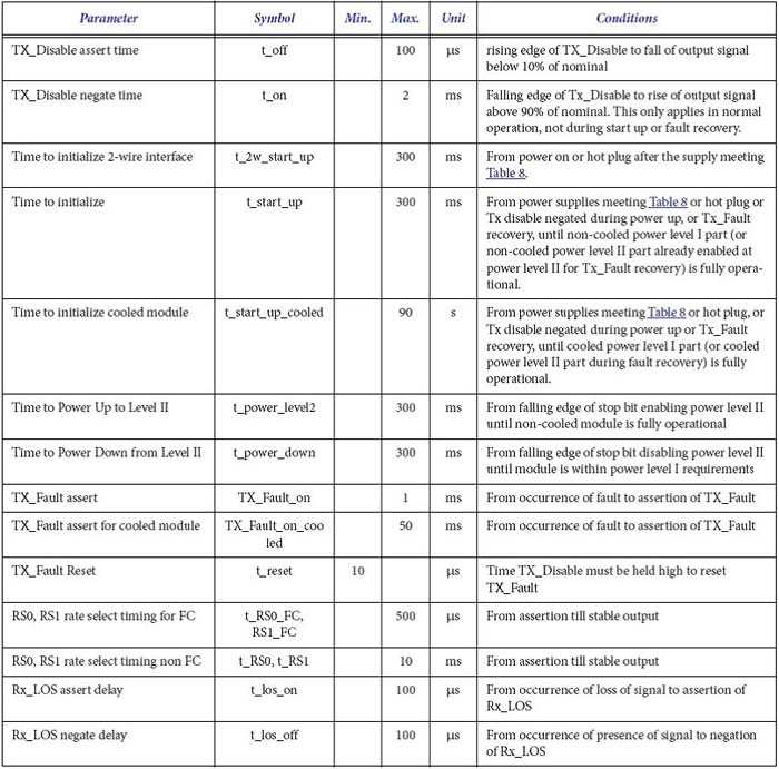
Table 8: Timing Characteristics
Mechanical
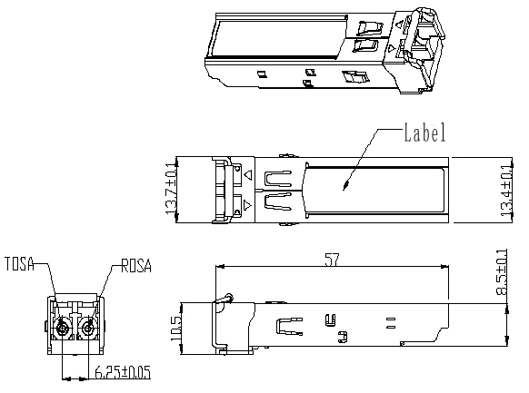
Table 9: Key Mechanical Dimensions
ESD
This transceiver is specified as ESD threshold 2kV for all electrical input pins, tested per MIL-STD-883, Method 3015.4 /JESD22-A114-A (HBM). However, normal ESD precautions are still required during the handling of this module. This transceiver is shipped in ESD protective packaging. It should be removed from the packaging and handled only in an ESD protected environment.
LASER SAFTY
This is a Class 1 Laser Product according to IEC 60825-1:1993:+A1:1997+A2:2001. This product complies with 21 CFR 1040.10 and 1040.11 except for deviations pursuant to Laser Notice No. 50, dated (July 26, 2001)
Ordering information
|
Part Number |
Product Description |
|
SPT-SFP-8G-SR |
850nm, 1.0625/2.125/4.25/8.5Gbs, 150m, 0ºC ~ +70ºC |
E-mail: sales@sopto.com
Web : http://www.sopto.com